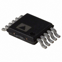
AD5243BRMZ10-RL7 Analog Devices Inc, AD5243BRMZ10-RL7 Datasheet - Page 16

AD5243BRMZ10-RL7
Manufacturer Part Number
AD5243BRMZ10-RL7
Description
IC,Digital Potentiometer,TSSOP,10PIN,PLASTIC
Manufacturer
Analog Devices Inc
Datasheet
1.AD5243BRMZ2.5.pdf
(20 pages)
Specifications of AD5243BRMZ10-RL7
Taps
256
Resistance (ohms)
10K
Number Of Circuits
2
Temperature Coefficient
35 ppm/°C Typical
Memory Type
Volatile
Interface
I²C, 2-Wire Serial
Voltage - Supply
2.7 V ~ 5.5 V
Operating Temperature
-40°C ~ 125°C
Mounting Type
Surface Mount
Package / Case
10-MSOP, Micro10™, 10-uMAX, 10-uSOP
Resistance In Ohms
10K
Lead Free Status / RoHS Status
Lead free / RoHS Compliant
For Use With
AD5243EVAL - BOARD EVAL FOR AD5243
Lead Free Status / RoHS Status
Lead free / RoHS Compliant
AD5243/AD5248
I
I
The 2-wire, I
1.
2.
2
2
C COMPATIBLE, 2-WIRE SERIAL BUS
C INTERFACE
The master initiates data transfer by establishing a start
condition, which is when a high-to-low transition on the
SDA line occurs while SCL is high (see Figure 46). The
following byte is the slave address byte, which consists of
the slave address followed by an R/ W bit (this bit deter-
mines whether data is read from or written to the slave
device). The AD5243 has a fixed slave address byte,
whereas the AD5248 has two configurable address bits,
AD0 and AD1 (see
The slave whose address corresponds to the transmitted
address responds by pulling the SDA line low during the
ninth clock pulse (this is called the acknowledge bit). At
this stage, all other devices on the bus remain idle while the
selected device waits for data to be written to or read from
its serial register. If the R/ W bit is high, the master reads
from the slave device. On the other hand, if the R/ W bit is
low, the master writes to the slave device.
In the write mode, the second byte is the instruction byte.
The first bit (MSB) of the instruction byte is the RDAC
subaddress select bit. A logic low selects Channel 1 and a
logic high selects Channel 2.
The second MSB, SD, is a shutdown bit. A logic high causes
an open circuit at Terminal A while shorting the wiper to
Terminal B. This operation yields almost 0 Ω in rheostat
mode or 0 V in potentiometer mode. It is important to
note that the shutdown operation does not disturb the
contents of the register. When the AD5243 or AD5248 is
brought out of shutdown, the previous setting is applied to
the RDAC. In addition, during shutdown, new settings can
be programmed. When the part is returned from shutdown,
the corresponding VR setting is applied to the RDAC.
The remainder of the bits in the instruction byte are don’t
care bits (see Figure 10).
After acknowledging the instruction byte, the last byte in
write mode is the data byte. Data is transmitted over the
serial bus in sequences of nine clock pulses (eight data bits
followed by an acknowledge bit). The transitions on the
2
C-compatible serial bus protocol operates as follows:
Figure 10
).
Rev. A | Page 16 of 20
3.
4.
SDA line must occur during the low period of SCL and
remain stable during the high period of SCL (see Figure 46
and Figure 47).
In the read mode, the data byte follows immediately after the
acknowledgment of the slave address byte. Data is transmitted
over the serial bus in sequences of nine clock pulses (a slight
difference with the write mode, where there are eight data bits
followed by an acknowledge bit). Similarly, the transitions
on the SDA line must occur during the low period of SCL and
remain stable during the high period of SCL (see Figure 48
and Figure 49).
Note that the channel of interest is the one that is previously
selected in write mode. If users need to read the RDAC
values of both channels, they need to program the first
channel in write mode and then change to read mode to
read the first channel value. After that, the user must return
the device to write mode with the second channel selected
and read the second channel value in read mode. It is not
necessary for users to issue the Frame 3 data byte in write
mode for subsequent readback operation. Users should refer
to Figure 48 and Figure 49 for the programming format.
After all data bits have been read or written, a stop condition
is established by the master. A stop condition is defined as
a low-to-high transition on the SDA line while SCL is high.
In write mode, the master pulls the SDA line high during
the 10
46 and Figure 47). In read mode, the master issues a no
acknowledge for the ninth clock pulse (that is, the SDA line
remains high). The master then brings the SDA line low
before the 10
stop condition (see Figure 48 and Figure 49).
A repeated write function provides the user with the flexibility
of updating the RDAC output multiple times after addressing
and instructing the part only once. For example, after the
RDAC has acknowledged its slave address and instruction
bytes in write mode, the RDAC output updates on each
successive byte. If different instructions are needed, however,
the write/read mode must restart with a new slave address,
instruction, and data byte. Similarly, a repeated read function
of the RDAC is also allowed.
th
clock pulse to establish a stop condition (see Figure
th
clock pulse, which goes high to establish a


