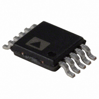
AD5243BRMZ10-RL7 Analog Devices Inc, AD5243BRMZ10-RL7 Datasheet - Page 3

AD5243BRMZ10-RL7
Manufacturer Part Number
AD5243BRMZ10-RL7
Description
IC,Digital Potentiometer,TSSOP,10PIN,PLASTIC
Manufacturer
Analog Devices Inc
Datasheet
1.AD5243BRMZ2.5.pdf
(20 pages)
Specifications of AD5243BRMZ10-RL7
Taps
256
Resistance (ohms)
10K
Number Of Circuits
2
Temperature Coefficient
35 ppm/°C Typical
Memory Type
Volatile
Interface
I²C, 2-Wire Serial
Voltage - Supply
2.7 V ~ 5.5 V
Operating Temperature
-40°C ~ 125°C
Mounting Type
Surface Mount
Package / Case
10-MSOP, Micro10™, 10-uMAX, 10-uSOP
Resistance In Ohms
10K
Lead Free Status / RoHS Status
Lead free / RoHS Compliant
For Use With
AD5243EVAL - BOARD EVAL FOR AD5243
Lead Free Status / RoHS Status
Lead free / RoHS Compliant
SPECIFICATIONS
ELECTRICAL CHARACTERISTICS: 2.5 kΩ VERSION
V
Table 1.
Parameter
DC CHARACTERISTICS—RHEOSTAT MODE
DC CHARACTERISTICS—POTENTIOMETER
RESISTOR TERMINALS
DIGITAL INPUTS AND OUTPUTS
POWER SUPPLIES
DYNAMIC CHARACTERISTICS
1
2
3
4
5
6
7
8
9
10
Typical specifications represent average readings at 25°C and V
Resistor position nonlinearity error, R-INL, is the deviation from an ideal value measured between the maximum resistance and the minimum resistance wiper
positions. R-DNL measures the relative step change from the ideal between successive tap positions. Parts are guaranteed monotonic.
V
Specifications apply to all VRs.
INL and DNL are measured at V
DNL specification limits of ±1 LSB maximum are guaranteed monotonic operating conditions.
Resistor Terminal A, Resistor Terminal B, and Resistor Terminal W have no limitations on polarity with respect to each other.
Guaranteed by design, but not subject to production test.
Measured at the A terminal. The A terminal is open circuited in shutdown mode.
P
All dynamic characteristics use V
DD
A
DISS
Resistor Differential Nonlinearity
Resistor Integral Nonlinearity
Nominal Resistor Tolerance
Resistance Temperature Coefficient
Wiper Resistance
DIVIDER MODE
Differential Nonlinearity
Integral Nonlinearity
Voltage Divider Temperature Coefficient
Full-Scale Error
Zero-Scale Error
Voltage Range
Capacitance A, B
Capacitance W
Shutdown Supply Current
Common-Mode Leakage
Input Logic High
Input Logic Low
Input Logic High
Input Logic Low
Input Current
Input Capacitance
Power Supply Range
Supply Current
Power Dissipation
Power Supply Sensitivity
Bandwidth, −3 dB
Total Harmonic Distortion
V
Resistor Noise Voltage Density
= V
W
= 5 V ± 10%, or 3 V ± 10%; V
is calculated from (I
Settling Time
DD
, V
B
= 0 V, wiper (V
6
7
4
7
9
7
DD
W
5
× V
) = no connect.
W
DD
5
with the RDAC configured as a potentiometer divider similar to a voltage output digital-to-analog converter (DAC). V
). CMOS logic level inputs result in minimum power dissipation.
8
DD
10
3
= 5 V.
2
A
2
= V
DD
; V
B
Symbol
R-DNL
R-INL
∆R
(∆R
R
DNL
INL
(∆V
V
V
V
C
C
I
I
V
V
V
V
I
C
V
I
P
PSS
BW
THD
t
e
= 0 V; −40°C < T
A_SD
CM
IL
DD
S
N_WB
WB
WFSE
WZSE
A
A
W
IH
IL
IH
IL
IL
DD RANGE
DISS
, V
, C
AB
AB
W
W
B
/V
B
/R
, V
W
AB
W
DD
)/∆T
)/∆T
= 5 V.
Rev. A | Page 3 of 20
Conditions
R
R
T
V
Code = 0x00, V
Code = 0x80
Code = 0xFF
Code = 0x00
f = 1 MHz, measured to GND,
code = 0x80
f = 1 MHz, measured to GND,
code = 0x80
V
V
V
V
V
V
V
V
V
V
Code = 0x80
V
V
R
A
A
WB
WB
AB
DD
A
DD
DD
DD
DD
IN
IH
IH
DD
A
A
WB
< +125°C; unless otherwise noted.
= 25°C
= V
= 1 V rms, V
= 5 V, V
= 0 V or 5 V
= 5 V or V
= 5 V or V
, V
, V
= V
= 5.5 V
= 5 V
= 5 V
= 3 V
= 3 V
= 5 V ± 10%, code = midscale
= 1.25 kΩ, R
A
A
B
DD
= no connect
= no connect
= V
, wiper = no connect
B
DD
= 0 V, ±1 LSB error band
/2
IL
IL
= 0 V
= 0 V, V
B
DD
= 0 V, f = 1 kHz
S
= 0
= 5 V
DD
= 5 V
Min
−2
−14
−20
−1.5
−2
−14
0
GND
2.4
2.1
2.7
Typ
±0.1
±2
35
160
±0.1
±0.6
15
−5.5
4.5
45
60
0.01
1
5
3.5
±0.02
4.8
0.1
1
3.2
AD5243/AD5248
1
A
= V
DD
Max
+2
+14
+55
200
+1.5
+2
0
12
V
1
0.8
0.6
±1
5.5
6
30
±0.08
and V
DD
B
= 0 V.
Unit
LSB
LSB
%
ppm/°C
Ω
LSB
LSB
ppm/°C
LSB
LSB
V
pF
pF
μA
nA
V
V
V
V
μA
pF
V
μA
μW
%/%
MHz
%
μs
nV/√Hz


