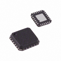
AD7147ACPZ-1REEL Analog Devices Inc, AD7147ACPZ-1REEL Datasheet - Page 11

AD7147ACPZ-1REEL
Manufacturer Part Number
AD7147ACPZ-1REEL
Description
IC,Converter, Other/Special/Miscellaneous,LLCC,24PIN
Manufacturer
Analog Devices Inc
Series
CapTouch™r
Type
Capacitive Sensor Controllerr
Datasheet
1.AD7147ACPZ-1500RL7.pdf
(72 pages)
Specifications of AD7147ACPZ-1REEL
Resolution (bits)
16 b
Data Interface
I²C, Serial
Voltage Supply Source
Single Supply
Voltage - Supply
2.6 V ~ 3.6 V
Operating Temperature
-40°C ~ 85°C
Mounting Type
Surface Mount
Package / Case
24-LFCSP
Lead Free Status / RoHS Status
Lead free / RoHS Compliant
For Use With
EVAL-AD7147EBZ - BOARD EVAL FOR AD7147ACPZEVAL-AD7147-1EBZ - BOARD EVAL FOR AD7147ACPZ-1
Sampling Rate (per Second)
-
Lead Free Status / RoHS Status
Lead free / RoHS Compliant
THEORY OF OPERATION
The AD7147 and AD7147-1 are CDCs with on-chip environ-
mental compensation. They are intended for use in portable
systems requiring high resolution user input. The internal
circuitry consists of a 16-bit, ∑-Δ converter that can change a
capacitive input signal into a digital value. There are 13 input
pins, CIN0 to CIN12, on the AD7147 or AD7147-1. A switch
matrix routes the input signals to the CDC. The result of each
capacitance-to-digital conversion is stored in on-chip registers.
The host subsequently reads the results over the serial interface.
The AD7147 has an SPI interface, and the AD7147-1 has an I
interface, ensuring that the parts are compatible with a wide
range of host processors. AD7147 refers to both the AD7147
and AD7147-1, unless otherwise noted, from this point forward
in this data sheet.
The AD7147 interfaces with up to 13 external capacitance
sensors. These sensors can be arranged as buttons, scroll bars,
or wheels, or as a combination of sensor types. The external
sensors consist of an electrode on a single- or multiple-layer
PCB that interfaces directly to the AD7147.
The AD7147 can be set up to implement any set of input
sensors by programming the on-chip registers. The registers
can also be programmed to control features such as averaging,
offsets, and gains for each of the external sensors. There is an
on-chip sequencer that controls how each of the capacitance
inputs is polled.
The AD7147 has on-chip digital logic and 528 words of RAM
that are used for environmental compensation. The effects of
humidity, temperature, and other environmental factors can
affect the operation of capacitance sensors. Transparent to the
user, the AD7147 performs continuous calibration to compen-
sate for these effects, allowing the AD7147 to consistently
provide error-free results.
The AD7147 requires a companion algorithm that runs on the
host or another microcontroller to implement high resolution
sensor functions, such as scroll bars or wheels. However, no
companion algorithm is required to implement buttons. Button
sensors are implemented on chip, entirely in digital logic.
The AD7147 can be programmed to operate in either full power
mode or low power automatic wake-up mode. The automatic
wake-up mode is particularly suited for portable devices that
Rev. B | Page 11 of 72
2
C
require low power operation to provide the user with significant
power savings and full functionality.
The AD7147 has an interrupt output, INT , to indicate when
new data has been placed into the registers. INT is used to
interrupt the host on sensor activation. The AD7147 operates
from a 2.6 V to 3.6 V supply and is available in a 24-lead, 4 mm ×
4 mm LFCSP.
CAPACITANCE SENSING THEORY
The AD7147 measures capacitance changes from single electrode
sensors. The sensor electrode on the PCB comprises one plate
of a virtual capacitor. The other plate of the capacitor is the user’s
finger, which is grounded with respect to the sensor input.
The AD7147 first outputs an excitation signal to charge the
plate of the capacitor. When the user comes close to the sensor,
the virtual capacitor is formed, with the user acting as the second
capacitor plate.
A square wave excitation signal is applied to CINx during
the conversion, and the modulator continuously samples the
charge going through CINx. The output of the modulator is
processed via a digital filter, and the resulting digital data is
stored in the CDC_RESULT_Sx registers for each conversion
stage, at Address 0x00B to Address 0x016.
AD7147
Figure 19. Capacitance-Sensing Method
SENSOR PCB
ADC
Σ-Δ
PLASTIC COVER
EXCITATION
SIGNAL
250kHz
16-BIT
DATA
AD7147


