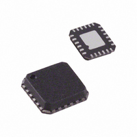
AD7147PACPZ-1RL Analog Devices Inc, AD7147PACPZ-1RL Datasheet - Page 36

AD7147PACPZ-1RL
Manufacturer Part Number
AD7147PACPZ-1RL
Description
CAPACITANCE TO DIGITAL CONVERTER
Manufacturer
Analog Devices Inc
Series
CapTouch™r
Type
Capacitive Sensor Controllerr
Datasheet
1.AD7147ACPZ-1500RL7.pdf
(72 pages)
Specifications of AD7147PACPZ-1RL
Resolution (bits)
16 b
Data Interface
I²C, Serial
Voltage Supply Source
Single Supply
Voltage - Supply
2.6 V ~ 3.6 V
Operating Temperature
-40°C ~ 85°C
Mounting Type
Surface Mount
Package / Case
24-LFCSP
Lead Free Status / RoHS Status
Lead free / RoHS Compliant
Sampling Rate (per Second)
-
Lead Free Status / Rohs Status
Compliant
AD7147
Writing Data over the I
The process for writing to the AD7147-1 over the I
shown in Figure 53 and Figure 55. The device address is sent
over the bus, followed by the R/ W bit being set to 0 and then
two bytes of data that contain the 10-bit address of the internal
data register to be written. The following bit map shows the
upper register address bytes. Note that Bit 7 to Bit 2 in the upper
address byte are don’t care bits. The address is contained in the
10 LSBs of the register address bytes.
MSB
7
X
The following bit map shows the lower register address bytes.
MSB
7
Reg
Add
Bit 7
The third data byte contains the eight MSBs of the data to be
written to the internal register. The fourth data byte contains
the eight LSBs of data to be written to the internal register.
The AD7147-1 address pointer register automatically increments
after each write. This allows the master to sequentially write to all
registers on the AD7147-1 in the same write transaction. However,
the address pointer register does not wrap around after the last
SCLK
SDA
START
NOTES
1. A START CONDITION AT THE BEGINNING IS DEFINED AS A HIGH-TO-LOW TRANSITION ON SDA WHILE SCLK REMAINS HIGH.
2. A STOP CONDITION AT THE END IS DEFINED AS A LOW-TO-HIGH TRANSITION ON SDA WHILE SCLK REMAINS HIGH.
3. 7-BIT DEVICE ADDRESS [DEV A6:DEV A0] = [0 1 0 1 1 X X], WHERE X IS A DON’T CARE BIT.
4. 16-BIT REGISTER ADDRESS [A15:A0] = [X, X, X, X, X, X, A9, A8, A7, A6, A5, A4, A3, A2, A1, A0], WHERE X IS A DON’T CARE BIT.
5. REGISTER ADDRESS [A15:A8] AND REGISTER ADDRESS [A7:A0] ARE ALWAYS SEPARATED BY A LOW ACK BIT.
6. REGISTER DATA [D15:D8] AND REGISTER DATA [D7:D0] ARE ALWAYS SEPARATED BY A LOW ACK BIT.
6
X
6
Reg
Add
Bit 6
ACK
27
D15
t
1
5
X
28
5
Reg
Add
Bit 5
DEV
A6
REGISTER DATA [D15:D8]
D14
1
29
DEV
AD7147-1 DEVICE ADDRESS
4
X
A5
2
4
Reg
Add
Bit 4
2
C Bus
DEV
A4
3
3
X
DEV
A3
t
3
Reg
Add
Bit 3
2
D9
4
34
DEV
2
X
A2
D8
t
5
4
Figure 53. Example of I
35
2
Reg
Add
Bit 2
DEV
A1
ACK
6
1
Register
Address
Bit 9
t
36
3
DEV
A0
D7
7
1
Reg
Add
Bit 1
2
37
C bus is
R/W
REGISTER DATA [D7:D0]
D6
8
38
0
Register
Address
Bit 8
t
5
ACK
0
Reg
Add
Bit 0
9
2
C Timing for Single Register Write Operation
LSB
LSB
Rev. B | Page 36 of 72
A15
10
REGISTER ADDRESS [A15:A8]
A14
D1
11
43
address. Therefore, any data written to the AD7147-1 after the
address pointer has reached its maximum value is discarded.
All registers on the AD7147-1 are 16 bits. Two consecutive 8-bit
data bytes are combined and written to the 16-bit registers. To
avoid errors, all writes to the device must contain an even
number of data bytes.
To finish the transaction, the master generates a stop condition
on SDO, or generates a repeat start condition if the master is to
maintain control of the bus.
Reading Data over the I
To read from the AD7147-1, the address pointer register must
first be set to the address of the required internal register. The
master performs a write transaction, and then writes to the
AD7147-1 to set the address pointer. Next, the master outputs a
repeat start condition to keep control of the bus, or if this is not
possible, ends the write transaction with a stop condition. A read
transaction is initiated, with the R/ W bit set to 1.
The AD7147-1 supplies the upper eight bits of data from the
addressed register in the first readback byte, followed by the
lower eight bits in the next byte. This is shown in Figure 54 and
Figure 55.
Because the address pointer automatically increments after each
read, the AD7147-1 continues to output readback data until the
master sends a no acknowledge and stop condition to the bus. If
the address pointer reaches its maximum value and the master
continues to read from the part, the AD7147-1 repeatedly sends
data from the last register that was addressed.
D0
44
ACK
45
A9
16
46
STOP
t
6
A8
17
ACK
t
18
8
A7
START
19
t
REGISTER ADDRESS [A7:A0]
7
2
C Bus
A6
20
DEV
AD7147-1 DEVICE ADDRESS
A6
1
DEV
A5
A1
2
25
DEV
A4
A0
3
26


