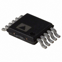
AD7789BRM Analog Devices Inc, AD7789BRM Datasheet - Page 11

AD7789BRM
Manufacturer Part Number
AD7789BRM
Description
Low Power 24-Bit SD ADC I.C.
Manufacturer
Analog Devices Inc
Datasheet
1.AD7789BRMZ.pdf
(20 pages)
Specifications of AD7789BRM
Rohs Status
RoHS non-compliant
Number Of Bits
24
Sampling Rate (per Second)
16.6
Data Interface
DSP, MICROWIRE™, QSPI™, Serial, SPI™
Number Of Converters
1
Power Dissipation (max)
230µW
Voltage Supply Source
Single Supply
Operating Temperature
-40°C ~ 105°C
Mounting Type
Surface Mount
Package / Case
10-TFSOP (0.118", 3.00mm Width)
Lead Free Status / RoHS Status
Contains lead / RoHS non-compliant
Available stocks
Company
Part Number
Manufacturer
Quantity
Price
Part Number:
AD7789BRMZ
Manufacturer:
ADI/亚德诺
Quantity:
20 000
ON-CHIP REGISTERS
The ADC is controlled and configured via a number of on-chip
registers, which are described on the following pages. In the
following descriptions, set implies a Logic 1 state and cleared
implies a Logic 0 state, unless otherwise stated.
COMMUNICATIONS REGISTER
(RS1, RS0 = 0, 0)
The communications register is an 8-bit, write only register. All
communications to the part must start with a write operation to
the communications register. The data written to the commun-
ications register determines whether the next operation is a read
or write operation, and to which register this operation takes
place.
CR7
WEN[0]
Table 7. Communications Register Bit Designations
Bit Location
CR7
CR6
CR5 to CR4
CR3
CR2
CR1 to CR0
Bit Name
WEN
0
RS1 to RS0
R/W
CREAD
CH1 to CH0
CR6
0[0]
Description
Write Enable Bit. A 0 must be written to this bit so that the write to the communications register actually
occurs. If a 1 is the first bit written, the part does not clock on to subsequent bits in the register. It stays at
this bit location until a 0 is written to this bit. Once a 0 is written to the WEN bit, the next seven bits are
loaded to the communications register.
This bit must be programmed with a Logic 0 for correct operation.
Register Address Bits. These address bits are used to select which of the ADC registers are being selected
during this serial interface communication (see Table 8).
A 0 in this bit location indicates that the next operation is a write to a specified register. A 1 in this position
indicates that the next operation is a read from the designated register.
Continuous Read of the Data Register. When this bit is set to 1 (and the data register is selected), the serial
interface is configured so that the data register can be continuously read, that is, the contents of the data
register are placed on the DOUT/RDY pin automatically when the SCLK pulses are applied. The
communications register does not have to be written to for data reads. To enable continuous read mode,
the instruction 001111XX must be written to the communications register. To exit the continuous read
mode, the instruction 001110XX must be written to the communications register while the DOUT/RDY pin
is low. While in continuous read mode, the ADC monitors activity on the DIN line so that it can receive the
instruction to exit continuous read mode. Additionally, a reset occurs if 32 consecutive 1s are seen on DIN.
Therefore, DIN should be held low in continuous read mode until an instruction is to be written to the
device.
These bits are used to select the analog input channel. The differential channel can be selected
AIN(+)/AIN(−) or an internal short AIN(−)/AIN(−) can be selected. Alternatively, the power supply can be
selected, that is, the ADC can measure the voltage on the power supply, which is useful for monitoring
power supply variation. The power supply voltage is divided by 5 and then applied to the modulator for
conversion. The ADC uses a 1.17 V ± 5% on-chip reference as the reference source for the analog-to-digital
conversion. Any change in channel resets the filter and a new conversion is started.
CR5
RS1[0]
CR4
RS0[0]
Rev. B | Page 11 of 20
CR3
R/W[0]
For read or write operations, once the subsequent read or write
operation to the selected register is complete, the interface returns
to where it expects a write operation to the communications
register. This is the default state of the interface and, on power-up
or after a reset, the ADC is in this default state waiting for a write
operation to the communications register. In situations where the
interface sequence is lost, a write operation of at least 32 serial
clock cycles with DIN high returns the ADC to this default state
by resetting the entire part. Table 7 outlines the bit designations
for the communications register. CR0 through CR7 indicate the
bit location, CR denoting the bits are in the communications
register. CR7 denotes the first bit of the data stream. The number
in brackets indicates the power-on/reset default status of that bit.
CR2
CREAD[0]
CR1
CH1[0]
AD7788/AD7789
CR0
CH0[0]


