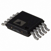
AD7789BRM Analog Devices Inc, AD7789BRM Datasheet - Page 9

AD7789BRM
Manufacturer Part Number
AD7789BRM
Description
Low Power 24-Bit SD ADC I.C.
Manufacturer
Analog Devices Inc
Datasheet
1.AD7789BRMZ.pdf
(20 pages)
Specifications of AD7789BRM
Rohs Status
RoHS non-compliant
Number Of Bits
24
Sampling Rate (per Second)
16.6
Data Interface
DSP, MICROWIRE™, QSPI™, Serial, SPI™
Number Of Converters
1
Power Dissipation (max)
230µW
Voltage Supply Source
Single Supply
Operating Temperature
-40°C ~ 105°C
Mounting Type
Surface Mount
Package / Case
10-TFSOP (0.118", 3.00mm Width)
Lead Free Status / RoHS Status
Contains lead / RoHS non-compliant
Available stocks
Company
Part Number
Manufacturer
Quantity
Price
Part Number:
AD7789BRMZ
Manufacturer:
ADI/亚德诺
Quantity:
20 000
PIN CONFIGURATION AND FUNCTION DESCRIPTIONS
Table 6. Pin Function Descriptions
Pin No.
1
2
3
4
5
6
7
8
9
10
Mnemonic
SCLK
CS
AIN(+)
AIN(−)
REFIN(+)
REFIN(−)
GND
V
DOUT/RDY
DIN
DD
Description
Serial Clock Input for Data Transfers to and from the ADC. The SCLK has a Schmitt-triggered input, making the
interface suitable for opto-isolated applications. The serial clock can be continuous, with all data transmitted in
a continuous train of pulses. Alternatively, it can be a noncontinuous clock with the information being trans-
mitted to or from the ADC in smaller batches of data.
Chip Select Input. This is an active low logic input used to select the ADC. CS can be used to select the ADC in
systems with more than one device on the serial bus or as a frame synchronization signal in communicating
with the device. CS can be hardwired low, allowing the ADC to operate in 3-wire mode with SCLK, DIN, and
DOUT/RDY used to interface with the device.
Analog Input. AIN(+) is the positive terminal of the fully differential analog input.
Analog Input. AIN(–) is the negative terminal of the fully differential analog input.
Positive Reference Input. REFIN(+) can lie anywhere between V
voltage (REFIN(+)
Negative Reference Input. This reference input can lie anywhere between GND and V
Ground Reference Point.
Supply Voltage. 3 V or 5 V nominal.
The DOUT/RDY falling edge can be used as an interrupt to a processor, indicating that valid data is available.
With an external serial clock, the data can be read using the DOUT/RDY pin. With CS low, the data/control word
information is placed on the DOUT/RDY pin on the SCLK falling edge and is valid on the SCLK rising edge.
The end of a conversion is also indicated by the RDY bit in the status register. When CS is high, the DOUT/RDY
pin is three-stated, but the RDY bit remains active.
Serial Data Input to the Input Shift Register on the ADC. Data in this shift register is transferred to the control
registers within the ADC; the register selection bits of the communications register identify the appropriate
register.
−
REFIN(−)) is 2.5 V, but the part functions with a reference from 0.1 V to V
REFIN(+)
AIN(+)
AIN(–)
SCLK
CS
Figure 5. Pin Configuration
1
2
3
4
5
Rev. B | Page 9 of 20
(Not to Scale)
AD7788/
AD7789
TOP VIEW
10
9
8
7
6
DIN
DOUT/RDY
V
GND
REFIN(–)
DD
DD
and GND + 0.1 V. The nominal reference
DD
− 0.1 V.
AD7788/AD7789
DD
.


