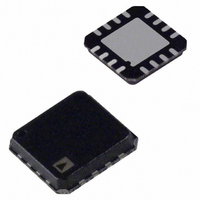
AD7879-1ACPZ-500R7 Analog Devices Inc, AD7879-1ACPZ-500R7 Datasheet - Page 35

AD7879-1ACPZ-500R7
Manufacturer Part Number
AD7879-1ACPZ-500R7
Description
Touch Screen Controller
Manufacturer
Analog Devices Inc
Type
Resistiver
Datasheet
1.AD7879-1ACPZ-500R7.pdf
(40 pages)
Specifications of AD7879-1ACPZ-500R7
Touch Panel Interface
4-Wire
Number Of Inputs/keys
1 TSC
Resolution (bits)
12 b
Data Interface
I²C, Serial
Data Rate/sampling Rate (sps, Bps)
105k
Voltage Reference
External
Voltage - Supply
1.6 V ~ 3.6 V
Current - Supply
10nA
Operating Temperature
-40°C ~ 85°C
Mounting Type
Surface Mount
Package / Case
16-LFCSP-VQ
Voltage Supply Source
Single Supply
Sampling Rate (per Second)
105k
Lead Free Status / RoHS Status
Lead free / RoHS Compliant
Other names
AD7879-1ACPZ-500R7TR
Available stocks
Company
Part Number
Manufacturer
Quantity
Price
Company:
Part Number:
AD7879-1ACPZ-500R7
Manufacturer:
AD
Quantity:
4 957
Writing Data over the I
The process of writing to the AD7879-1/AD7889-1 over the I
bus is shown in Figure 43 and Figure 45. The device address is
sent over the bus followed by the R/ W bit set to 0. This is followed
by one byte of data that contains the 8-bit address of the internal
data register to be written. The bit map in Table 26 shows the
register address byte.
Table 26. I
MSB
7
Bit 7
The third data byte contains the eight MSBs of the data to be
written to the internal register. The fourth data byte contains
the eight LSBs of data to be written to the internal register.
The AD7879-1/AD7889-1 address pointer register automatically
increments after each write. This allows the master to sequentially
write to all registers on the AD7879-1/AD7889-1 in the same
write transaction. However, the address pointer register does
not wrap after the last address.
Any data written to the AD7879-1/AD7889-1 after the address
pointer has reached its maximum value is discarded.
6
Bit 6
2
C Register Address Byte
SDA
SCL
START
NOTES
1. A START CONDITION AT THE BEGINNING IS DEFINED AS A HIGH-TO-LOW TRANSITION ON SDA WHILE SCL REMAINS HIGH.
2. A STOP CONDITION AT THE END IS DEFINED AS A LOW-TO-HIGH TRANSITION ON SDA WHILE SCL REMAINS HIGH.
3. 7-BIT DEVICE ADDRESS [DEV A6:DEV A0] = [01011XX], WHERE THE Xs ARE DON'T CARE BITS.
4. REGISTER DATA [D15:D8] AND REGISTER DATA [D7:D0] ARE ALWAYS SEPARATED BY A LOW ACK BIT.
5
Bit 5
ACK
18
AD7879-1/AD7889-1 DEVICE ADDRESS
D15
Register Address
t
1
19
REGISTER DATA[D15:D8]
4
Bit 4
2
DEV
C Bus
A6
D14
1
20
DEV
A5
2
3
Bit 3
DEV
A4
3
DEV
A3
t
2
D9
Figure 43. Example of I
4
25
2
Bit 2
DEV
A2
D8
t
5
4
26
DEV
A1
ACK
6
t
27
3
1
Bit 1
DEV
A0
D7
7
28
REGISTER DATA[D7:D0]
R/W
D6
8
29
t
5
0
Bit 0
ACK
2
Rev. C | Page 35 of 40
C Timing for Single Register Write Operation
LSB
9
2
C
A7
10
REGISTER ADDRESS[A7:A0]
A6
D1
11
34
D0
All registers on the AD7879-1/AD7889-1 have 16 bits. Two
consecutive 8-bit data bytes are combined and written to the
16-bit registers. To avoid errors, all writes to the device must
contain an even number of data bytes.
To end the transaction, the master generates a stop condition on
SDA, or it generates a repeat start condition if the master is to
maintain control of the bus.
Reading Data over the I
To read from the AD7879-1/AD7889-1, the address pointer
register must first be set to the address of the required internal
register. The master performs a write transaction and writes to
the AD7879-1/AD7889-1 to set the address pointer. The master
then outputs a repeat start condition to keep control of the bus
or, if this is not possible, the master ends the write transaction
with a stop condition. A read transaction is initiated, with the
R/ W bit set to 1.
The AD7879-1/AD7889-1 supply the upper eight bits of data
from the addressed register in the first readback byte, followed
by the lower eight bits in the next byte. This is shown in Figure 44
and Figure 45.
Because the address pointer automatically increments after each
read, the AD7879-1/AD7889-1 continue to output readback data
until the master puts a no acknowledge and a stop condition on
the bus. If the address pointer reaches its maximum value and
the master continues to read from the part, the AD7879-1/
AD7889-1 repeatedly send data from the last register addressed.
35
ACK
36
A1
16
37
STOP
t
6
A0
17
t
8
START
t
7
2
C Bus
AD7879-1/AD7889-1
DEVICE ADDRESS
DEV
A6
1
DEV
A5
2
AD7879/AD7889
DEV
A4
3


