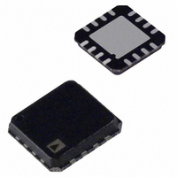
AD7879-1ACPZ-500R7 Analog Devices Inc, AD7879-1ACPZ-500R7 Datasheet - Page 37

AD7879-1ACPZ-500R7
Manufacturer Part Number
AD7879-1ACPZ-500R7
Description
Touch Screen Controller
Manufacturer
Analog Devices Inc
Type
Resistiver
Datasheet
1.AD7879-1ACPZ-500R7.pdf
(40 pages)
Specifications of AD7879-1ACPZ-500R7
Touch Panel Interface
4-Wire
Number Of Inputs/keys
1 TSC
Resolution (bits)
12 b
Data Interface
I²C, Serial
Data Rate/sampling Rate (sps, Bps)
105k
Voltage Reference
External
Voltage - Supply
1.6 V ~ 3.6 V
Current - Supply
10nA
Operating Temperature
-40°C ~ 85°C
Mounting Type
Surface Mount
Package / Case
16-LFCSP-VQ
Voltage Supply Source
Single Supply
Sampling Rate (per Second)
105k
Lead Free Status / RoHS Status
Lead free / RoHS Compliant
Other names
AD7879-1ACPZ-500R7TR
Available stocks
Company
Part Number
Manufacturer
Quantity
Price
Company:
Part Number:
AD7879-1ACPZ-500R7
Manufacturer:
AD
Quantity:
4 957
For detailed information on grounding and layout considerations
for the AD7879/AD7889, refer to the AN-577 Application Note,
Layout and Grounding Recommendations for Touch Screen
Digitizers.
LEAD FRAME CHIP SCALE PACKAGES
The lands on the lead frame chip scale package (CP-16-10) are
rectangular. The printed circuit board (PCB) pad for these lands
should be 0.1 mm longer than the package land length and
0.05 mm wider than the package land width. Center the land on
the pad to maximize the solder joint size.
The bottom of the lead frame chip scale package has a central
thermal pad. The thermal pad on the PCB should be at least as
large as this exposed pad. To avoid shorting, provide a clearance
GROUNDING AND LAYOUT
SCREEN
TOUCH
NC = NO CONNECT
1
2
3
4
NC
NC
Y+
X–
Figure 46. Typical Application Circuit
AD7879/
AD7889
PENIRQ/INT/DAV
Rev. C | Page 37 of 40
0.1µF
DOUT
NC
NC
of at least 0.25 mm between the thermal pad and the inner
edges of the land pattern on the PCB. Thermal vias can be used
on the PCB thermal pad to improve the thermal performance of
the package. If vias are used, incorporate them into the thermal
pad at a 1.2 mm pitch grid. The via diameter should be between
0.3 mm and 0.33 mm, and the via barrel should be plated with
1 oz. of copper to plug the via.
Connect the PCB thermal pad to GND.
WLCSP ASSEMBLY CONSIDERATIONS
For detailed information on the WLCSP PCB assembly and
reliability, see the AN-617 Application Note, MicroCSP™ Wafer
Level Chip Scale Package.
12
11
10
9
0.1µF TO 10µF
(OPTIONAL)
CS
INT
SCLK
MISO
MOSI
REGULATOR
VOLTAGE
HOST
MAIN
BATTERY
AD7879/AD7889


