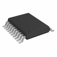
AD9834BRU Analog Devices Inc, AD9834BRU Datasheet - Page 9

AD9834BRU
Manufacturer Part Number
AD9834BRU
Description
10 Bit, 20 Pin DDS I.C.
Manufacturer
Analog Devices Inc
Datasheet
1.AD9834BRUZ.pdf
(36 pages)
Specifications of AD9834BRU
Rohs Status
RoHS non-compliant
Design Resources
Amplitude Control Circuit for AD9834 Waveform Generator (CN0156)
Resolution (bits)
10 b
Master Fclk
50MHz
Tuning Word Width (bits)
28 b
Voltage - Supply
2.3 V ~ 5.5 V
Operating Temperature
-40°C ~ 105°C
Mounting Type
Surface Mount
Package / Case
20-TSSOP
Lead Free Status / RoHS Status
Contains lead / RoHS non-compliant
For Use With
EVAL-AD9834EBZ - BOARD EVAL FOR AD9834
Lead Free Status / RoHS Status
Contains lead / RoHS non-compliant
Available stocks
Company
Part Number
Manufacturer
Quantity
Price
Part Number:
AD9834BRU
Manufacturer:
ADI/亚德诺
Quantity:
20 000
Part Number:
AD9834BRUZ
Manufacturer:
ADI/亚德诺
Quantity:
20 000
Company:
Part Number:
AD9834BRUZ-REEL
Manufacturer:
AD
Quantity:
1 045
Part Number:
AD9834BRUZ-REEL
Manufacturer:
ADI/亚德诺
Quantity:
20 000
Pin No.
13
14
15
16
Mnemonic
SDATA
SCLK
FSYNC
SIGN BIT
OUT
Description
Serial Data Input. The 16-bit serial data-word is applied to this input.
Serial Clock Input. Data is clocked into the AD9834 on each falling SCLK edge.
Active Low Control Input. This is the frame synchronization signal for the input data. When FSYNC is taken low, the
internal logic is informed that a new word is being loaded into the device.
Logic Output. The comparator output is available on this pin or, alternatively, the MSB from the NCO can be output
on this pin. Setting Bit OPBITEN in the control register to 1 enables this output pin. Bit SIGN/PIB determines
whether the comparator output or the MSB from the NCO is output on the pin.
Rev. C | Page 9 of 36
AD9834


