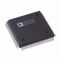
AD9887AKSZ-140 Analog Devices Inc, AD9887AKSZ-140 Datasheet - Page 14

AD9887AKSZ-140
Manufacturer Part Number
AD9887AKSZ-140
Description
IC,TV/VIDEO CIRCUIT,Video Digitizer,CMOS,QFP,160PIN,PLASTIC
Manufacturer
Analog Devices Inc
Datasheet
1.AD9887AKSZ-140.pdf
(52 pages)
Specifications of AD9887AKSZ-140
Applications
Graphic Cards, VGA Interfaces
Interface
Analog and Digital
Voltage - Supply
3.15 V ~ 3.45 V
Package / Case
160-MQFP, 160-PQFP
Mounting Type
Surface Mount
Lead Free Status / RoHS Status
Lead free / RoHS Compliant
Available stocks
Company
Part Number
Manufacturer
Quantity
Price
Company:
Part Number:
AD9887AKSZ-140
Manufacturer:
MAX
Quantity:
59
Company:
Part Number:
AD9887AKSZ-140
Manufacturer:
ADI
Quantity:
364
Company:
Part Number:
AD9887AKSZ-140
Manufacturer:
Analog Devices Inc
Quantity:
10 000
Part Number:
AD9887AKSZ-140
Manufacturer:
ADI/亚德诺
Quantity:
20 000
AD9887A
CKINV
Sync Outputs
HSOUT
SOGOUT Sync-on-Green Slicer Output
Voltage References
REFOUT Internal Reference Output
Sampling Clock Inversion (Optional)
This pin can be used to invert the pixel sampling
clock, which has the effect of shifting the sampling
phase 180°. This supports the alternate pixel
sampling mode, wherein higher frequency input
signals (up to 340 MPPS) can be captured by
sampling the odd pixels and capturing the even
pixels on the subsequent frame.
This pin should be used only during blanking
intervals (typically vertical blanking), because it
might produce several samples of corrupted data
during the phase shift.
CKINV should be grounded when not used.
Either or both signals can be used, depending on
the timing mode and the interface design used.
Horizontal Sync Output
A reconstructed, phase-aligned version of the HSYNC
input. Both the polarity and duration of this output
can be programmed via serial bus registers.
By maintaining alignment with DATACK,
DATACK , and Data, data timing with respect to
horizontal sync can be determined.
This pin can be programmed to output either the
composite sync output from the sync-on-green slicer
comparator or an unprocessed, but delayed, version
of the HSYNC input. See the sync processing block
diagram (Figure 43) to see how this pin is connected.
This is the output from the internal 1.25 V band gap
reference. This output is intended to drive relatively
light loads. It can drive the AD9887A reference input
directly, but should be externally buffered if it is used
to drive other loads, as well.
The absolute accuracy of this output is ±4%, and the
temperature coefficient is ±50 ppm, which is adequate
for most AD9887A applications. If higher accuracy
is required, an external reference can be used instead.
When using an external reference, connect this pin
to ground through a 0.1 μF capacitor.
Rev. B | Page 14 of 52
REFIN
PLL Filter
FILT
Data Outputs
RED A
RED B
GREEN A Data Output, Green Channel, Port A/Even
GREEN B Data Output, Green Channel, Port B/Odd
BLUE A
BLUE B
Reference Input
The reference input accepts the master reference
voltage for all AD9887A internal circuitry (1.25 V ±
10%). It can be driven directly by the REFOUT pin.
Its high impedance presents a very light load to the
reference source.
This pin should always be bypassed to ground with
a 0.1 μF capacitor.
External Filter Connection
For proper operation, the pixel clock generator, PLL,
requires an external filter. Connect the filter shown
in Figure 11 to this pin. For optimal performance,
minimize noise and parasitics on this node.
Data Output, Red Channel, Port A/Even
Data Output, Red Channel, Port B/Odd
Data Output, Blue Channel, Port A/Even
Data Output, Blue Channel, Port B/Odd
These are the main data outputs. Bit 7 is the MSB.
Each channel has two ports. When the part is operated
in single-channel mode (DEMUX = 0), all data
presented to Port A and Port B is placed in a high
impedance state. Programming demux to 1 establishes
the dual-channel mode, wherein alternate pixels are
presented to the Port A and Port B of each channel.
These appear simultaneously; two pixels are presented
at the time of every second input pixel when PAR is
set to 1 (parallel mode). When PAR is set to 0, pixel
data appears alternately on the two ports, one new
sample with each incoming pixel (interleaved mode).
In dual-channel mode, the first pixel after Hsync is
routed to Port A. The second pixel goes to Port B,
the third to Port A, and so on.
The delay from pixel sampling time to output is
fixed. When the sampling time is changed by adjusting
the PHASE register, the output timing is shifted as well.
The DATACK, DATACK , and HSOUT outputs are
also moved; therefore, the timing relationship among
the signals is maintained.


