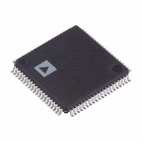
AD9980KSTZ-80 Analog Devices Inc, AD9980KSTZ-80 Datasheet - Page 13

AD9980KSTZ-80
Manufacturer Part Number
AD9980KSTZ-80
Description
IC,Data Acquisition Signal Conditioner,3-CHANNEL,8-BIT,CMOS,QFP,80PIN,PLASTIC
Manufacturer
Analog Devices Inc
Datasheet
1.AD9980KSTZ-80.pdf
(44 pages)
Specifications of AD9980KSTZ-80
Applications
Video
Interface
Analog
Voltage - Supply
3.13 V ~ 3.47 V
Package / Case
80-LQFP
Mounting Type
Surface Mount
Lead Free Status / RoHS Status
Lead free / RoHS Compliant
For Use With
AD9980/PCBZ - KIT EVALUATION AD9980
Lead Free Status / RoHS Status
Lead free / RoHS Compliant
Available stocks
Company
Part Number
Manufacturer
Quantity
Price
Company:
Part Number:
AD9980KSTZ-80
Manufacturer:
ADI
Quantity:
830
Company:
Part Number:
AD9980KSTZ-80
Manufacturer:
Analog Devices Inc
Quantity:
10 000
Part Number:
AD9980KSTZ-80
Manufacturer:
ADI/亚德诺
Quantity:
20 000
Any jitter in the clock reduces the precision with which the
sampling time can be determined and must also be subtracted
from the stable pixel time. Considerable care has been taken in
the design of the AD9980’s clock generation circuit to minimize
jitter. The clock jitter of the AD9980 is 9% or less of the total
pixel time in all operating modes, making the reduction in the
valid sampling time due to jitter negligible.
The PLL characteristics are determined by the loop filter design,
the PLL Charge Pump Current, and the VCO range setting. The
loop filter design is illustrated in Figure 7. Recommended
settings of VCO range and charge pump current for VESA
standard display modes are listed in Table 9.
Four programmable registers are provided to optimize the
performance of the PLL. These registers are
1.
2.
The 12-Bit Divisor Register. The input Hsync frequencies
can accommodate any Hsync as long as the product of the
Hsync and the PLL divisor falls within the operating range
of the VCO. The PLL multiplies the frequency of the Hsync
signal, producing pixel clock frequencies in the range of
10 MHz to 95 MHz. The divisor register controls the exact
multiplication factor. This register may be set to any value
between 2 and 4095 as long as the output frequency is
within range.
The 2-Bit VCO Range Register. To improve the noise
performance of the AD9980, the VCO operating frequency
range is divided into four overlapping regions. The VCO
PIXEL CLOCK
8nF
C
P
Figure 6. Pixel Sampling Times
Figure 7. PLL Loop Filter Detail
FILT
INVALID SAMPLE TIMES
1.5kΩ
R
Z
C
80nF
Z
PV
D
Rev. 0 | Page 13 of 44
Table 7. VCO Frequency Ranges
PV1
0
0
1
1
3.
Table 8. Charge Pump Current/Control Bits
Ip2
0
0
0
0
1
1
1
1
4.
range register sets this operating range. The frequency
ranges for the four regions are shown in Table 7.
The 3-bit Charge Pump Current Register. This register
varies the current that drives the low-pass loop filter. The
possible current values are listed in Table 8.
The 5-bit Phase Adjust Register. The phase of the generated
sampling clock may be shifted to locate an optimum samp-
ling point within a clock cycle. The phase adjust register
provides 32 phase-shift steps of 11.25° each. The Hsync
signal with an identical phase shift is available through the
HSOUT pin. Phase adjust is still available if an external
pixel clock is used. The COAST pin or internal Coast is
used to allow the PLL to continue to run at the same
frequency in the absence of the incoming Hsync signal or
during disturbances in Hsync (such as from equalization
pulses). This may be used during the vertical sync period
or at any other time that the Hsync signal is unavailable.
The polarity of the Coast signal may be set through the
Coast polarity register (Register 0x18, Bits [6:5]). Also, the
polarity of the Hsync signal may be set through the Hsync
polarity register (Register 0x12, Bits [5:4]). For both Hsync
and Coast, a value of 1 is active high. The internal Coast
function is driven off of the Vsync signal, which is typically
a time when Hsync signals may be disrupted with extra
equalization pulses.
PV0
0
1
0
1
Ip1
0
0
1
1
0
0
1
1
Pixel Clock
Range (MHz)
10 to 21
21 to 42
42 to 84
84 to 95
Ip0
0
1
0
1
0
1
0
1
Current (µA)
50
100
150
250
350
500
750
1500
KVCO
Gain (MHz/V)
150
150
150
150
AD9980


