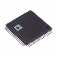
AD9980KSTZ-80 Analog Devices Inc, AD9980KSTZ-80 Datasheet - Page 33

AD9980KSTZ-80
Manufacturer Part Number
AD9980KSTZ-80
Description
IC,Data Acquisition Signal Conditioner,3-CHANNEL,8-BIT,CMOS,QFP,80PIN,PLASTIC
Manufacturer
Analog Devices Inc
Datasheet
1.AD9980KSTZ-80.pdf
(44 pages)
Specifications of AD9980KSTZ-80
Applications
Video
Interface
Analog
Voltage - Supply
3.13 V ~ 3.47 V
Package / Case
80-LQFP
Mounting Type
Surface Mount
Lead Free Status / RoHS Status
Lead free / RoHS Compliant
For Use With
AD9980/PCBZ - KIT EVALUATION AD9980
Lead Free Status / RoHS Status
Lead free / RoHS Compliant
Available stocks
Company
Part Number
Manufacturer
Quantity
Price
Company:
Part Number:
AD9980KSTZ-80
Manufacturer:
ADI
Quantity:
830
Company:
Part Number:
AD9980KSTZ-80
Manufacturer:
Analog Devices Inc
Quantity:
10 000
Part Number:
AD9980KSTZ-80
Manufacturer:
ADI/亚德诺
Quantity:
20 000
0x1B
Table 37. Auto-Offset Settings
Auto-Offset
0
1
0x1B
Table 38. Auto-Offset Update Mode
Clamp Update
00
01
10
11
0x1B
0x1C
SOG CONTROL
0x1D
0x1D
Table 39. SOGOUT Polarity Settings
SOGOUT
0
1
0x1D
5
This bit selects between auto-offset mode and manual
offset mode (auto-offset disabled). See the section on
auto-offset operation. The power-up default setting
is 0.
4:3
These bits control how often the auto-offset circuit is
updated (if enabled). Updating every 64 Hsyncs is
recommended. The power-up default setting is 11.
2:0
7:0
Must be written to 0xFF for proper operation.
7:3
This register allows the comparator threshold of the
SOG slicer to be adjusted. This register adjusts it in
steps of 8 mV, with the minimum setting equaling
8 mV and the maximum setting equaling 256 mV. The
power-up default setting is 15 and corresponds to a
threshold value of 128 mV.
2
This bit sets the polarity of the SOGOUT signal. The
power-up default setting is 0.
1:0
These register bits control the output on the SOGOUT
pin. Options are the raw SOG from the slicer (this is
the unprocessed SOG signal produced from the sync
slicer), the raw Hsync, the regenerated sync from the
sync filter that can generate missing syncs either due
to coasting or dropout, and the filtered sync which
Auto-Offset Enable
Auto-Offset Update Frequency
Must be written to 011 for proper operation.
TestReg0
SOG Comparator Threshold
SOG Output Polarity
SOG Output Select
Result
Active low
Active high
Result
Update offset every clamp period
Update offset every 16 clamp periods
Update offset every 64 clamp periods
Update offset every Vsync periods
Result
Auto-offset is disabled
Auto-offset is enabled (manual offset
mode)
Rev. 0 | Page 33 of 44
Table 40. SOGOUT Polarity Settings
SOGOUT Select
00
01
10
11
INPUT AND POWER CONTROL
0x1E
Table 41. Channel Source Override
Override
0
1
0x1E
Table 42. Channel Select
Channel Select
0
1
0x1E
Table 43. Input Bandwidth Select
Input Bandwidth
0
1
0x1E
excludes extraneous syncs not occurring within the
sync filter window. The power-up default setting is 0.
7
This bit provides an override to the automatic input
channel selection. Power-up default setting is 0.
6
This bit selects the active input channel if
Register 0x1E, Bit 7 = 1. This selects between
Channel 0 data and syncs or Channel 1 data and
syncs. Power-up default setting is 0.
5
This bit selects between a low or high input
bandwidth. It is useful in limiting noise for lower
frequency inputs. The power-up default setting is 1.
Low analog input bandwidth is ~100 MHz; high
analog input bandwidth is ~200 MHz.
4
This bit sets whether power-down is controlled
manually or automatically by the chip. If automatic
control is selected (0x1E, Bit 4), the AD9980’s decision
is based on the status of the sync detect bits (Register
0x24, Bits 2, 3, 6, and 7). If either an Hsync or a sync-
on-green input is detected on any input, the chip
powers up, otherwise it powers down. If manual
control is desired, the AD9980 includes flexibility of
control with both a dedicated pin and a register bit.
The dedicated pin allows a hardware watchdog circuit
to control power-down, while the register bit allows
Result
Channel input source determined by chip
Channel input source determined by user
Register 0x1E, Bit 6
Channel Select Override
Channel Select
Programmable Bandwidth
Power-Down Control Select
Result
Channel 0 data and syncs are selected
Channel 1 data and syncs are selected
Function
Raw SOG from sync slicer (SOG0 or SOG1)
Raw Hsync (Hsync0 or Hsync1)
Regenerated sync from sync filter
Filtered sync from sync filter
Result
Low analog input bandwidth
High analog input bandwidth
AD9980


