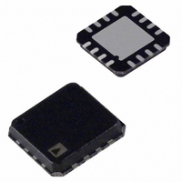
ADA4939-1YCPZ-R2 Analog Devices Inc, ADA4939-1YCPZ-R2 Datasheet - Page 17

ADA4939-1YCPZ-R2
Manufacturer Part Number
ADA4939-1YCPZ-R2
Description
IC,Differential Amplifier,SINGLE,BIPOLAR,LLCC,16PIN,PLASTIC
Manufacturer
Analog Devices Inc
Datasheet
1.ADA4939-1YCPZ-R7.pdf
(24 pages)
Specifications of ADA4939-1YCPZ-R2
Amplifier Type
Differential
Number Of Circuits
1
Output Type
Differential
Slew Rate
6800 V/µs
-3db Bandwidth
1.4GHz
Current - Input Bias
10µA
Voltage - Input Offset
500µV
Current - Supply
36.5mA
Current - Output / Channel
100mA
Voltage - Supply, Single/dual (±)
3 V ~ 5.25 V, ±1.5 V ~ 2.625 V
Operating Temperature
-40°C ~ 105°C
Mounting Type
Surface Mount
Package / Case
16-LFCSP
Lead Free Status / RoHS Status
Lead free / RoHS Compliant
Gain Bandwidth Product
-
Lead Free Status / RoHS Status
Lead free / RoHS Compliant
THEORY OF OPERATION
The ADA4939 differs from conventional op amps in that it has
two outputs whose voltages move in opposite directions and an
additional input, V
loop gain and negative feedback to force these outputs to the
desired voltages. The ADA4939 behaves much like a standard
voltage feedback op amp and facilitates single-ended-to-differential
conversions, common-mode level shifting, and amplifications of
differential signals. Like an op amp, the ADA4939 has high input
impedance and low output impedance. Because it uses voltage
feedback, the ADA4939 manifests a nominally constant gain-
bandwidth product.
Two feedback loops are employed to control the differential and
common-mode output voltages. The differential feedback, set
with external resistors, controls only the differential output voltage.
The common-mode feedback controls only the common-mode
output voltage. This architecture makes it easy to set the output
common-mode level to any arbitrary value within the specified
limits. The output common-mode voltage is forced, by the internal
common-mode feedback loop, to be equal to the voltage applied
to the V
The internal common-mode feedback loop produces outputs
that are highly balanced over a wide frequency range without
requiring tightly matched external components. This results in
differential outputs that are very close to the ideal of being
identical in amplitude and are exactly 180° apart in phase.
ANALYZING AN APPLICATION CIRCUIT
The ADA4939 uses high open-loop gain and negative feedback
to force its differential and common-mode output voltages in
such a way as to minimize the differential and common-mode
error voltages. The differential error voltage is defined as the
voltage between the differential inputs labeled +IN and −IN
(see Figure 42). For most purposes, this voltage can be assumed
to be zero. Similarly, the difference between the actual output
common-mode voltage and the voltage applied to V
be assumed to be zero. Starting from these two assumptions,
any application circuit can be analyzed.
OCM
input.
OCM
. Like an op amp, it relies on high open-
OCM
can also
Rev. 0 | Page 17 of 24
SETTING THE CLOSED-LOOP GAIN
The differential-mode gain of the circuit in Figure 42 can be
determined by
This presumes that the input resistors (R
(R
STABLE FOR GAINS ≥2
The ADA4939 frequency response exhibits excessive peaking
for differential gains <2; therefore, the part should be operated
with differential gains ≥2.
ESTIMATING THE OUTPUT NOISE VOLTAGE
The differential output noise of the ADA4939 can be estimated
using the noise model in Figure 43. The input-referred noise
voltage density, v
noise currents, i
ground. The output voltage due to v
v
follows). The noise currents are uncorrelated with the same
mean-square value, and each produces an output voltage that is
equal to the noise current multiplied by the associated feedback
resistance. The noise voltage density at the V
When the feedback networks have the same feedback factor, as
in most cases, the output noise due to v
Each of the four resistors contributes (4kTR
from the feedback resistors appears directly at the output, and
the noise from the gain resistors appears at the output multiplied
by R
multiplication factors, and the output-referred noise density terms.
nIN
F
) on each side are equal.
by the noise gain, G
F
/R
V
V
OUT
G
IN
. Table 11 summarizes the input noise sources, the
,
,
dm
dm
V
V
nRG1
nRG2
=
nIN−
R
R
nIN
R
R
G
F
i
i
G1
G2
, is modeled as a differential input, and the
nIN+
nIN–
and i
Figure 43. Noise Model
N
nIN+
(defined in the G
V
nIN
ADA4939-1/ADA4939-2
, appear between each input and
R
R
F1
F2
ADA4939
+
nIN
V
V
V
nRF1
OCM
nRF2
is obtained by multiplying
G
nCM
) and feedback resistors
N
is common-mode.
xx
equation that
V
OCM
)
nOD
1/2
V
nCM
. The noise
pin is v
nCM
.


