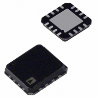
ADA4939-1YCPZ-R2 Analog Devices Inc, ADA4939-1YCPZ-R2 Datasheet - Page 20

ADA4939-1YCPZ-R2
Manufacturer Part Number
ADA4939-1YCPZ-R2
Description
IC,Differential Amplifier,SINGLE,BIPOLAR,LLCC,16PIN,PLASTIC
Manufacturer
Analog Devices Inc
Datasheet
1.ADA4939-1YCPZ-R7.pdf
(24 pages)
Specifications of ADA4939-1YCPZ-R2
Amplifier Type
Differential
Number Of Circuits
1
Output Type
Differential
Slew Rate
6800 V/µs
-3db Bandwidth
1.4GHz
Current - Input Bias
10µA
Voltage - Input Offset
500µV
Current - Supply
36.5mA
Current - Output / Channel
100mA
Voltage - Supply, Single/dual (±)
3 V ~ 5.25 V, ±1.5 V ~ 2.625 V
Operating Temperature
-40°C ~ 105°C
Mounting Type
Surface Mount
Package / Case
16-LFCSP
Lead Free Status / RoHS Status
Lead free / RoHS Compliant
Gain Bandwidth Product
-
Lead Free Status / RoHS Status
Lead free / RoHS Compliant
ADA4939-1/ADA4939-2
2.
3.
2V p-p
V
1.09V p-p
S
It can be seen from Figure 47 that the effective R
upper feedback loop is now greater than the R
lower loop due to the addition of the termination resistors.
To compensate for the imbalance of the gain resistors,
a correction resistor (R
lower loop. R
source resistance R
is equal to R
R
1 V p-p, which was obtained with R
circuit with the Thevenin equivalent of the terminated source
and R
Figure 49 presents a tractable circuit with matched
feedback loops that can be easily evaluated.
In order to match the 50 Ω source resistance, the termi-
nation resistor, R
The closest standard 1% value for R
TS
Figure 49. Thevenin Equivalent and Matched Gain Resistors
V
= R
50Ω
R
TH
S
TS
2V p-p
TH
Figure 48. Calculating the Thevenin Equivalent
in the lower feedback loop is shown in Figure 49.
50Ω
R
V
= R
Figure 47. Adding Termination Resistor R
27.4Ω
27.4Ω
IN
S
R
60.4Ω
R
S
TH
||R
TS
TS
S
||R
R
50Ω
is equal to the Thevenin equivalent of the
T
R
T
S
.
T
T
200Ω
V
200Ω
, is calculated using R
R
R
= 27.4 Ω. Note that V
OCM
S
G
G
and the termination resistance R
200Ω
200Ω
V
R
R
OCM
R
60.4Ω
G
G
T
TS
) is added in series with R
400Ω
400Ω
ADA4939
R
R
F
F
+V
–V
400Ω
ADA4939
400Ω
1.09V p-p
R
R
S
S
F
F
+V
–V
S
S
V
T
T
TH
= 50 Ω. The modified
is 60.4 Ω.
T
TH
||300 Ω = 50 Ω.
27.4Ω
R
is greater than
TH
T
R
L
G
R
in the
V
L
G
OUT, dm
in the
G
V
in the
OUT, dm
T
and
Rev. 0 | Page 20 of 24
4.
2V p-p
Figure 50. Terminated Single-Ended-to-Differential System with G = 2
It is useful to point out two effects that occur with a
terminated input. The first is that the value of R
in both loops, lowering the overall closed-loop gain. The
second is that V
be if R
the output voltage, and for large resistor values in the feedback
loops (~1 kΩ), the effects essentially cancel each other out.
For small R
gain is not canceled completely by the increased V
can be seen by evaluating Figure 49.
The desired differential output in this example is 2 V p-p
because the terminated input signal was 1 V p-p and the
closed-loop gain = 2. The actual differential output voltage,
however, is equal to (1.09 V p-p)(400/227.4) = 1.92 V p-p.
To obtain the desired output voltage of 2 V p-p, a final gain
adjustment can be made by increasing R
any of the input circuitry. This is discussed in Step 4.
The feedback resistor value is modified as a final gain
adjustment to obtain the desired output voltage.
To make the output voltage V
calculated using the following formula:
The closest standard 1 % values to 417 Ω are 412 Ω and
422 Ω. Choosing 422 Ω gives a differential output voltage
of 2.02 V p-p.
The final circuit is shown in Figure 50.
R
V
(
F
Desired
S
=
50Ω
T
R
S
= 50 Ω. These two effects have opposite impacts on
V
F
OUT
1V p-p
60.4Ω
and R
V
27.4Ω
TH
R
R
,
dm
TS
T
TH
) (
is a little larger than 1 V p-p, as it would
G
R
, however, the diminished closed-loop
200Ω
200Ω
V
G
R
R
OCM
G
G
+
R
TS
) (
=
OUT
422Ω
422Ω
ADA4939
R
R
2
F
F
+V
–V
= 2 V p-p, R
V
. 1
P
S
S
−
09
P
F
)(
V
without modifying
227
P
−
P
4 .
G
Ω
F
is increased
must be
R
)
L
=
TH
V
2.02V p-p
417
OUT, dm
. This
Ω


