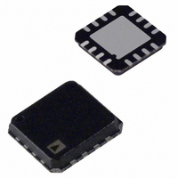
ADA4939-1YCPZ-R2 Analog Devices Inc, ADA4939-1YCPZ-R2 Datasheet - Page 19

ADA4939-1YCPZ-R2
Manufacturer Part Number
ADA4939-1YCPZ-R2
Description
IC,Differential Amplifier,SINGLE,BIPOLAR,LLCC,16PIN,PLASTIC
Manufacturer
Analog Devices Inc
Datasheet
1.ADA4939-1YCPZ-R7.pdf
(24 pages)
Specifications of ADA4939-1YCPZ-R2
Amplifier Type
Differential
Number Of Circuits
1
Output Type
Differential
Slew Rate
6800 V/µs
-3db Bandwidth
1.4GHz
Current - Input Bias
10µA
Voltage - Input Offset
500µV
Current - Supply
36.5mA
Current - Output / Channel
100mA
Voltage - Supply, Single/dual (±)
3 V ~ 5.25 V, ±1.5 V ~ 2.625 V
Operating Temperature
-40°C ~ 105°C
Mounting Type
Surface Mount
Package / Case
16-LFCSP
Lead Free Status / RoHS Status
Lead free / RoHS Compliant
Gain Bandwidth Product
-
Lead Free Status / RoHS Status
Lead free / RoHS Compliant
Mismatched feedback networks also result in a degradation of
the ability of the circuit to reject input common-mode signals,
much the same as for a four-resistor difference amplifier made
from a conventional op amp.
As a practical summarization of the above issues, resistors of 1%
tolerance produce a worst-case input CMRR of approximately
40 dB, a worst-case differential-mode output offset of 25 mV
due to a 2.5 V V
and no significant degradation in output balance error.
CALCULATING THE INPUT IMPEDANCE FOR AN
APPLICATION CIRCUIT
The effective input impedance of a circuit depends on whether
the amplifier is being driven by a single-ended or differential
signal source. For balanced differential input signals, as shown
in Figure 44, the input impedance (R
(+D
For an unbalanced, single-ended input signal (see Figure 45),
the input impedance is
IN
Figure 44. ADA4939 Configured for Balanced (Differential) Inputs
R
and −D
IN
Figure 45. ADA4939 with Unbalanced (Single-Ended) Input
,
SE
R
IN
+D
–D
=
, SE
⎛
⎜
⎜
⎜
⎜
⎝
IN
IN
IN
1
) is simply R
OCM
−
V
R
R
OCM
2
G
G
R
R
×
input, negligible V
G
G
R
(
R
G
R
G
V
F
OCM
+IN
+
–IN
R
ADA4939
IN, dm
ADA4939
R
R
F
F
F
+V
–V
)
+V
R
R
⎞
⎟
⎟
⎟
⎟
⎠
S
S
= 2 × R
F
S
F
IN, dm
OCM
G
) between the inputs
.
noise contribution,
V
R
OUT, dm
L
V
OUT, dm
Rev. 0 | Page 19 of 24
The input impedance of the circuit is effectively higher than it
would be for a conventional op amp connected as an inverter
because a fraction of the differential output voltage appears at
the inputs as a common-mode signal, partially bootstrapping
the voltage across the input resistor R
voltage at the amplifier input terminals can be easily determined by
noting that the voltage at the inverting input is equal to the
noninverting output voltage divided down by the voltage divider
formed by R
both input terminals due to negative voltage feedback and is in
phase with the input signal, thus reducing the effective voltage
across R
Terminating a Single-Ended Input
This section deals with how to properly terminate a single-
ended input to the ADA4939 with a gain of 2, R
R
output voltage of 1 V p-p and source resistance of 50 Ω illustrates
the four simple steps that must be followed. Note that because
the terminated output voltage of the source is 1 V p-p, the open
circuit output voltage of the source is 2 V p-p. The source shown
in Figure 46 indicates this open-circuit voltage.
1.
G
= 200 Ω. An example using an input source with a terminated
2V p-p
The input impedance must be calculated using the formula
R
IN
V
G
S
Figure 46. Calculating Single-Ended Input Impedance R
=
in the upper loop and partially bootstrapping R
⎛
⎜
⎜
⎜
⎜
⎝
1
F
50Ω
R
−
and R
S
2
×
300Ω
R
(
R
R
IN
G
G
R
G
in the lower loop. This voltage is present at
F
+
200Ω
200Ω
V
R
R
R
OCM
F
G
G
)
ADA4939-1/ADA4939-2
⎞
⎟
⎟
⎟
⎟
⎠
=
⎛
⎜
⎜
⎜
⎜
⎝
1
−
400Ω
400Ω
ADA4939
R
R
2
F
F
+V
–V
G
×
. The common-mode
S
S
(
200
200
400
+
400
F
= 400 Ω, and
R
)
L
⎞
⎟
⎟
⎟
⎟
⎠
=
V
G
IN
OUT, dm
.
300
Ω


