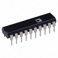
ADG333ABN Analog Devices Inc, ADG333ABN Datasheet - Page 3

ADG333ABN
Manufacturer Part Number
ADG333ABN
Description
Multiplexer IC
Manufacturer
Analog Devices Inc
Type
Analog Switchr
Datasheet
1.ADG333ABRZ.pdf
(12 pages)
Specifications of ADG333ABN
Peak Reflow Compatible (260 C)
No
Leakage Current
0.1nA
No. Of Circuits
4
Leaded Process Compatible
No
Mounting Type
Through Hole
No. Of Channels
4
On Resistance Rds(on)
20mohm
Package / Case
20-DIP
Rohs Status
RoHS non-compliant
Function
Switch
Circuit
4 x SPDT
On-state Resistance
45 Ohm
Voltage Supply Source
Single Supply
Voltage - Supply, Single/dual (±)
12V
Current - Supply
0.01µA
Operating Temperature
-40°C ~ 85°C
Package
20PDIP N
Maximum On Resistance
45@±15V Ohm
Maximum High Level Output Current
20 mA
Maximum Turn-off Time
100(Typ)@12V ns
Maximum Turn-on Time
110(Typ)@12V ns
Switch Architecture
SPDT
Power Supply Type
Single|Dual
Lead Free Status / RoHS Status
Contains lead / RoHS non-compliant
Available stocks
Company
Part Number
Manufacturer
Quantity
Price
Company:
Part Number:
ADG333ABN
Manufacturer:
Analog Devices Inc.
Quantity:
1 050
Part Number:
ADG333ABNZ
Manufacturer:
ADI/亚德诺
Quantity:
20 000
SPECIFICATIONS
DUAL SUPPLY
V
Table 1.
Parameter
ANALOG SWITCH
LEAKAGE CURRENTS
DIGITAL INPUTS
DYNAMIC CHARACTERISTICS
POWER REQUIREMENTS
1
2
Temperature range is as follows: B version: −40°C to +85°C.
Guaranteed by design; not subject to production test.
DD
Analog Signal Range
R
∆R
R
Source OFF Leakage I
Channel ON Leakage I
Input High Voltage, V
Input Low Voltage, V
Input Current
I
t
t
Break-Before-Make Delay, t
Charge Injection
OFF Isolation
Channel-to-Channel Crosstalk
C
C
I
I
V
INL
DD
SS
ON
OFF
ON
ON
DD
S
D
= +15 V, V
, C
(OFF)
ON
or I
/V
Match
S
SS
(ON)
INH
SS
= −15 V, GND = 0 V, unless otherwise noted.
INL
INH
S
D
(OFF)
, I
S
(ON)
2
OPEN
+25°C
20
45
±0.1
±0.25
±0.1
±0.4
90
80
10
2
10
72
85
7
26
0.05
0.25
0.01
1
−40°C to +85°C
V
45
5
4
±3
±5
2.4
0.8
±0.005
±0.5
175
145
0.35
5
±3/±20
SS
to V
Rev. A | Page 3 of 12
DD
1
V
Ω typ
Ω max
Ω max
Ω max
nA typ
nA max
nA typ
nA max
V min
V max
µA typ
µA max
ns typ
ns max
ns typ
ns max
ns min
pC typ
pC max
dB typ
dB typ
pF typ
pF typ
mA typ
mA max
µA typ
µA max
V min/V max
Unit
Test Conditions/Comments
V
V
V
V
V
Figure 15
V
Figure 16
V
R
V
R
V
R
V
V
V
R
V
R
V
Digital inputs = 0 V or 5 V
|V
L
L
L
L
L
D
D
D
DD
D
S
IN
S
S
S
D
DD
S
S
DD
= 300 Ω, C
= 300 Ω, C
= 300 Ω, C
= 75 Ω, C
= 75 Ω, C
= ±10 V, I
= V
= ±10 V; Figure 17
= ±10 V; Figure 17
= +5 V; Figure 18
= 2.3 V rms; Figure 20
= 2.3 V rms; Figure 21
= ±5 V, I
= ±10 V, I
= ±15.5 V, V
= 0 V, R
= 0 V or V
= +16.5 V, V
= +15 V, V
| = |V
D
= ±15.5 V
SS
D
|
S
L
L
= 0 Ω, C
S
= –10 mA
S
L
DD
L
L
= 5 pF, f = 1 MHz;
= 5 pF, f = 1 MHz;
= –1 mA
= –10 mA
= 35 pF;
= 35 pF;
= 35 pF;
SS
S
SS
= +15.5 V
= –15 V; Figure 19
= –16.5 V
L
= 10 nF;
ADG333A


