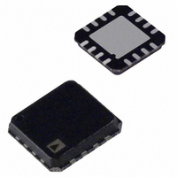
ADL5561ACPZ-R7 Analog Devices Inc, ADL5561ACPZ-R7 Datasheet

ADL5561ACPZ-R7
Specifications of ADL5561ACPZ-R7
Available stocks
Related parts for ADL5561ACPZ-R7
ADL5561ACPZ-R7 Summary of contents
Page 1
FEATURES −3 dB bandwidth of 2.9 GHz ( dB) V Low supply current Pin-strappable gain adjust: 6 dB, 12 dB, 15.5 dB Differential or single-ended input to differential output Low noise input stage: 2.1 nV/√Hz RTI ...
Page 2
ADL5561 TABLE OF CONTENTS Features .............................................................................................. 1 Applications ....................................................................................... 1 Functional Block Diagram .............................................................. 1 General Description ......................................................................... 1 Revision History ............................................................................... 2 Specifications ..................................................................................... 3 Absolute Maximum Ratings ............................................................ 6 ESD Caution .................................................................................. 6 Pin Configuration and Function Descriptions ...
Page 3
SPECIFICATIONS VCC = 3.3 V, VCOM = 1. 200 Ω differential Table 1. Parameter DYNAMIC PERFORMANCE −3 dB Bandwidth Bandwidth for 0.1 dB Flatness Gain Accuracy Gain Supply Sensitivity Gain Temperature Sensitivity Slew Rate Settling ...
Page 4
ADL5561 Parameter 10 MHz NOISE/HARMONIC PERFORMANCE Second/Third Harmonic Distortion Output Third-Order Intercept/Third-Order Intermodulation Distortion Noise Spectral Density (RTI Compression Point (RTO) 70 MHz NOISE/HARMONIC PERFORMANCE Second/Third Harmonic Distortion Output Third-Order Intercept/Third-Order Intermodulation Distortion Noise Spectral Density (RTI) 1 ...
Page 5
Parameter 250 MHz NOISE/HARMONIC PERFORMANCE Second/Third Harmonic Distortion Output Third-Order Intercept/Third-Order Intermodulation Distortion Noise Spectral Density (RTI Compression Point (RTO) 500 MHz NOISE/HARMONIC PERFORMANCE Second/Third Harmonic Distortion Output Third-Order Intercept/Third-Order Intermodulation Distortion Noise Spectral Density (RTI ...
Page 6
ADL5561 ABSOLUTE MAXIMUM RATINGS Table 2. Parameter Supply Voltage (VCC) VIP1, VIP2, VIN1, VIN2 Internal Power Dissipation θ JA Maximum Junction Temperature Operating Temperature Range Storage Temperature Range Stresses above those listed under Absolute Maximum Ratings may cause permanent damage ...
Page 7
PIN CONFIGURATION AND FUNCTION DESCRIPTIONS Table 3. Pin Function Descriptions Pin No. Mnemonic Description 1 VIP2 Balanced Differential Input. Biased to VCOM, typically ac-coupled. Input for A VIP1 for A 2 VIP1 Balanced Differential Input. Biased to VCOM, typically ac-coupled. ...
Page 8
ADL5561 TYPICAL PERFORMANCE CHARACTERISTICS VCC = 3.3 V, VCOM = 1. 200 Ω differential MAXIMUM GAIN 14 12 MID GAIN MINIMUM GAIN 4 10M 100M FREQUENCY (Hz) Figure 3. Gain vs. ...
Page 9
A MAXIMUM V A MID V A MINIMUM 100 150 FREQUENCY (MHz) Figure 9. Output Third-Order Intercept at Three Gains, Output Level p-p Composite 200 ...
Page 10
ADL5561 –40 –60 –80 –100 –120 –140 –160 0 50 100 150 FREQUENCY (MHz) Figure 15. Harmonic Distortion (HD2/HD3) vs. Frequency dB, and A = 15.5 dB, Output Level p- ...
Page 11
R (Ω) LOAD Figure 21. Harmonic Distortion (HD2/HD3) vs. R ENABLE 2V p-p OUTPUT TIME (2.5ns/DIV) Figure 22. ENBL Time Domain Response 2V p-p ...
Page 12
ADL5561 0 –10 –20 DISABLED –30 –40 ENABLED –50 –60 –70 0 0.5 1.0 1.5 FREQUENCY (GHz) Figure 27. Reverse Isolation (S12) vs. Frequency 1k A MAXIMUM V A MID 900 V A MINIMUM V 800 700 600 500 400 ...
Page 13
CIRCUIT DESCRIPTION BASIC STRUCTURE The ADL5561 is a low noise, low power, fully differential amplifier/ ADC driver that uses a 3.3 V supply. It provides three gain options (6 dB, 12 dB, and 15.5 dB) without the need for external ...
Page 14
ADL5561 APPLICATIONS INFORMATION BASIC CONNECTIONS Figure 31 shows the basic connections for operating the ADL5561. VCC should be 3.3 V with each supply pin decoupled with at least one low inductance surface-mount ceramic capacitor of 0.1 μF placed as close ...
Page 15
INPUT AND OUTPUT INTERFACING The ADL5561 can be configured as a differential input to differential output driver, as shown in Figure 32. The differential broadband input is provided by the ETC1-1-13 balun transformer, and the two 34.8 Ω resistors provide ...
Page 16
ADL5561 The single-ended gain can be determined using the following formula. The values of R and R for each gain configuration IN X are shown in Table 7. 400 × × ⎛ × ⎞ ...
Page 17
This circuit provides variable gain, isolation, and source matching for the AD9445. Using this circuit with the ADL5561 in a gain of 6 dB, an SFDR performance of 87 dBc is achieved at 140 MHz and a −3 dB bandwidth ...
Page 18
ADL5561 LAYOUT CONSIDERATIONS High-Q inductive drives and loads, as well as stray transmission line capacitance in combination with package parasitics, can potentially form a resonant circuit at high frequencies, resulting in excessive gain peaking or possible oscillation transmission ...
Page 19
SOLDERING INFORMATION On the underside of the chip scale package, there is an exposed compressed paddle. This paddle is internally connected to the ground of the chip. Solder the paddle to the low impedance ground plane on the PCB to ...
Page 20
ADL5561 Figure 44. Layout of Evaluation Board, Component Side Figure 45. Layout of Evaluation Board, Circuit Side Rev Page ...
Page 21
... OUTLINE DIMENSIONS PIN 1 INDICATOR 12° MAX 1.00 0.85 0.80 SEATING PLANE ORDERING GUIDE Temperature Model 1 Range ADL5561ACPZ-R7 −40°C to +85°C ADL5561ACPZ-WP −40°C to +85°C ADL5561-EVALZ RoHS Compliant Part. 3.00 0.60 MAX BSC SQ 0.45 12 2.75 TOP BSC SQ VIEW 9 0.50 BSC 1 ...
Page 22
ADL5561 NOTES Rev Page ...
Page 23
NOTES Rev Page ADL5561 ...
Page 24
ADL5561 NOTES ©2009–2010 Analog Devices, Inc. All rights reserved. Trademarks and registered trademarks are the property of their respective owners. D08004-0-3/10(B) Rev Page ...


