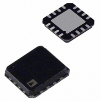
ADL5561ACPZ-R7 Analog Devices Inc, ADL5561ACPZ-R7 Datasheet - Page 17

ADL5561ACPZ-R7
Manufacturer Part Number
ADL5561ACPZ-R7
Description
Low Distortion 3V 41mA Diff Amp
Manufacturer
Analog Devices Inc
Datasheet
1.ADL5561ACPZ-R7.pdf
(24 pages)
Specifications of ADL5561ACPZ-R7
Amplifier Type
RF/IF Differential
Number Of Circuits
1
Output Type
Differential
Slew Rate
9800 V/µs
-3db Bandwidth
2.9GHz
Current - Input Bias
3µA
Current - Supply
40mA
Voltage - Supply, Single/dual (±)
3 V ~ 3.6 V
Operating Temperature
-40°C ~ 85°C
Mounting Type
Surface Mount
Package / Case
16-VFQFN, 16-CSP, Exposed Pad
Voltage - Supply
3 V ~ 3.6 V
Frequency
2.9GHz
Rf Type
General Purpose
Gain
15.5dB
Noise Figure
8dB
P1db
19dBm
Lead Free Status / RoHS Status
Lead free / RoHS Compliant
Test Frequency
-
Lead Free Status / RoHS Status
Lead free / RoHS Compliant
Other names
ADL5561ACPZ-R7TR
Available stocks
Company
Part Number
Manufacturer
Quantity
Price
Company:
Part Number:
ADL5561ACPZ-R7
Manufacturer:
MICREL
Quantity:
1 000
Part Number:
ADL5561ACPZ-R7
Manufacturer:
ADI/亚德诺
Quantity:
20 000
This circuit provides variable gain, isolation, and source matching
for the AD9445. Using this circuit with the ADL5561 in a gain
of 6 dB, an SFDR performance of 87 dBc is achieved at 140 MHz
and a −3 dB bandwidth of 760 MHz, as shown in Figure 38
and Figure 39.
Table 9. Interface Filter Recommendations for Various IF Sampling Frequencies
Center Frequency (MHz)
96
140
170
211
–100
–110
–120
–130
–140
–150
–10
–10
–20
–30
–40
–50
–60
–70
–80
–90
–1
–2
–3
–4
–5
–6
–7
–8
–9
0
2.00
0
Figure 39. Measured Frequency Response of the Wideband
0
Figure 38. Measured Single-Tone Performance of the
FIRST POINT = –1.12dBFS
END POINT = –4.38dBFS
MID POINT = –0.81dBFS
MIN = –4.38dBFS
MAX = –0.70dBFS
81.90
6.25 12.50 18.75 25.00 31.25 37.50 43.75 50.00 56.25 62.50
Circuit in Figure 37 for a 140 MHz Input Signal
161.80
241.70
ADL5561 DRIVING THE AD9445 14-BIT ADC
GAIN = 6dB
INPUT = 140MHz
SNR = 64.69dBc
SFDR = 87.44dBc
NOISE FLOOR = –107.9dB
FUND = –1.096dBFS
SECOND = –89.64dBc
THIRD = –87.52dBc
FREQUENCY (MHz)
FREQUENCY (MHz)
321.60
401.50
ADL5561
481.40
Figure 40. Narrow-Band IF Sampling Solution for an Unbuffered ADC Application
1 dB Bandwidth (MHz)
30
33
32
33
561.30
641.20
1nF
1nF
4Ω
4Ω
721.10
L1
L1
801.00
C2
L3
L3
Rev. B | Page 17 of 24
C4
105Ω
105Ω
L1 (nH)
3.3
3.3
3.3
3.3
The wideband frequency response is an advantage in broad-
band applications, such as predistortion receiver designs and
instrumentation applications. However, by designing for a wide
analog input frequency range, the cascaded SNR performance
is somewhat degraded due to high frequency noise aliasing into
the wanted Nyquist zone.
An alternative narrow-band approach is presented in Figure 40.
By designing a narrow band-pass antialiasing filter between the
ADL5561 and the target ADC, the output noise of the ADL5561
outside of the intended Nyquist zone can be attenuated, helping
to preserve the available SNR of the ADC. In general, the SNR
improves several decibels when including a reasonable order anti-
aliasing filter. In this example, a low loss 1:1 input transformer is
used to match the ADL5561 balanced input to a 50 Ω unbalanced
source, resulting in minimum insertion loss at the input.
Figure 40 is optimized for driving some of the Analog Devices
popular unbuffered ADCs, such as the AD9246, AD9640,
and AD6655. Table 9 includes antialiasing filter component
recommendations for popular IF sampling center frequencies.
Inductor L5 works in parallel with the on-chip ADC input
capacitance and a portion of the capacitance presented by C4 to
form a resonant tank circuit. The resonant tank helps to ensure
that the ADC input looks like a real resistance at the target center
frequency. The L5 inductor shorts the ADC inputs at dc, which
introduces a zero into the transfer function. In addition, the ac
coupling capacitors introduce additional zeros into the transfer
function. The final overall frequency response takes on a band-
pass characteristic, helping to reject noise outside of the intended
Nyquist zone. Table 9 provides initial suggestions for prototyping
purposes. Some empirical optimization may be needed to help
compensate for actual PCB parasitic.
CML
L5
C2 (pF)
47
47
56
47
AD9246
AD9640
AD6655
L3 (nH)
27
27
27
27
C4 (pF)
75
33
22
18
ADL5561
L5 (nH)
100
120
110
56


