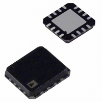
ADL5561ACPZ-R7 Analog Devices Inc, ADL5561ACPZ-R7 Datasheet - Page 14

ADL5561ACPZ-R7
Manufacturer Part Number
ADL5561ACPZ-R7
Description
Low Distortion 3V 41mA Diff Amp
Manufacturer
Analog Devices Inc
Datasheet
1.ADL5561ACPZ-R7.pdf
(24 pages)
Specifications of ADL5561ACPZ-R7
Amplifier Type
RF/IF Differential
Number Of Circuits
1
Output Type
Differential
Slew Rate
9800 V/µs
-3db Bandwidth
2.9GHz
Current - Input Bias
3µA
Current - Supply
40mA
Voltage - Supply, Single/dual (±)
3 V ~ 3.6 V
Operating Temperature
-40°C ~ 85°C
Mounting Type
Surface Mount
Package / Case
16-VFQFN, 16-CSP, Exposed Pad
Voltage - Supply
3 V ~ 3.6 V
Frequency
2.9GHz
Rf Type
General Purpose
Gain
15.5dB
Noise Figure
8dB
P1db
19dBm
Lead Free Status / RoHS Status
Lead free / RoHS Compliant
Test Frequency
-
Lead Free Status / RoHS Status
Lead free / RoHS Compliant
Other names
ADL5561ACPZ-R7TR
Available stocks
Company
Part Number
Manufacturer
Quantity
Price
Company:
Part Number:
ADL5561ACPZ-R7
Manufacturer:
MICREL
Quantity:
1 000
Part Number:
ADL5561ACPZ-R7
Manufacturer:
ADI/亚德诺
Quantity:
20 000
ADL5561
APPLICATIONS INFORMATION
BASIC CONNECTIONS
Figure 31 shows the basic connections for operating the ADL5561.
VCC should be 3.3 V with each supply pin decoupled with at least
one low inductance surface-mount ceramic capacitor of 0.1 μF
placed as close as possible to the device. The VCOM pin (Pin 9)
should also be decoupled using a 0.1 μF capacitor.
The gain of the part is determined by the pin-strappable input
configuration. When Input A is applied to VIP1 and Input B is
applied to VIN1, the gain is 6 dB (minimum gain; see Equation 1
and Equation 2). When Input A is applied to VIP2 and Input B is
applied to VIN2, the gain is 12 dB (middle gain). When Input A is
applied to VIP1 and VIP2 and Input B is applied to VIN1 and
VIN2, the gain is 15.5 dB (maximum gain).
BALANCED
SOURCE
R
R
S
S
/2
/2
0.1µF
0.1µF
A
B
Figure 31. Basic Connections
Rev. B | Page 14 of 24
1
2
3
4
VIP2
VIP1
VIN1
VIN2
10µF
ADL5561
Pin 1 to Pin 4, Pin 10, and Pin 11 are biased at 1/2 VCC above
ground and can be dc-coupled (if within the specified input and
output common-mode voltages levels) or ac-coupled, as shown
in Figure 31.
To enable the ADL5561, the ENBL pin must be pulled high.
Pulling the ENBL pin low puts the ADL5561 in sleep mode,
reducing the current consumption to 3 mA at ambient.
0.1µF
VCOM
ENBL
VON
VOP
12
10
11
9
VCC
0.1µF
R
L
BALANCED
LOAD


