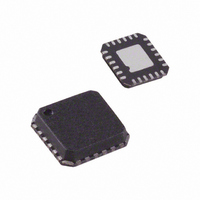
ADN8810ACPZ-REEL7 Analog Devices Inc, ADN8810ACPZ-REEL7 Datasheet - Page 11

ADN8810ACPZ-REEL7
Manufacturer Part Number
ADN8810ACPZ-REEL7
Description
Tunable Laser Controller
Manufacturer
Analog Devices Inc
Datasheet
1.ADN8810ACPZ-REEL7.pdf
(16 pages)
Specifications of ADN8810ACPZ-REEL7
Function
Current Source (12 Bit)
Current - Output
300mA
Operating Temperature
-40°C ~ 85°C
Mounting Type
Surface Mount
Package / Case
24-LFCSP
Lead Free Status / RoHS Status
Lead free / RoHS Compliant
Voltage - Input
-
Accuracy
-
Sensing Method
-
Lead Free Status / RoHS Status
Lead free / RoHS Compliant
FUNCTIONAL DESCRIPTION
The ADN8810 is a single 12-bit current output D/A converter
with a 3-wire SPI interface. Up to eight devices can be
independently programmed from the same SPI bus.
The full-scale output current is set with two external resistors.
The maximum output current can reach 300 mA. Figure 17
shows the functional block diagram of the ADN8810.
SETTING FULL-SCALE OUTPUT CURRENT
Two external resistors set the full-scale output current from the
ADN8810. These resistors are equal in value and are labeled R
in the Functional Block Diagram on the front page. Use 1% or
better tolerance resistors to achieve the most accurate output
current and the highest output impedance.
Equation 1 shows the approximate full-scale output current.
The exact output current is determined by the data register code
as shown in Equation 2. The variable code is an integer from 0
to 4095, representing the full 12-bit range of the ADN8810.
REFERENCE VOLTAGE SOURCE
The ADN8810 is designed to operate with a 4.096 V reference
voltage connected to VREF. The output current is directly
proportional to this reference voltage. A low noise precision
reference should be used to achieve the best performance. The
ADR292, ADR392, or REF198 is recommended.
POWER SUPPLIES
There are three principal supply current paths through the
ADN8810:
VREF
SCLK
I
I
FS
OUT
SDI
SB
CS
10
. 4
, 1
Code
DVDD
096
000
CONTROL
R
LOGIC
DGND
SN
BIAS
GEN
AVDD
R
Figure 17. Functional Block Diagram
1
SN
FAULT
ADDR2 ADDR1 ADDR0
R
15
DETECTION
SN
ADDRESS
DECODER
k
12-BIT
FAULT
DAC
0
DATA LATCH
1 .
12-BIT
RESET
FB
1.5k
ENCMP
15k
1.5k
DVSS
(1)
(2)
PVDD
PVDD
IOUT
IOUT
AVSS
R
SN
Rev. A | Page 11 of 16
SN
Current is returned through three pins:
For single-supply operation, set AVDD to 5 V, set PVDD from
3.0 V to 5 V, and connect AVSS, AGND, and DGND to ground.
SERIAL DATA INTERFACE
The ADN8810 uses a serial peripheral interface (SPI) with three
input signals: SDI, CLK, and CS . Figure 2 shows the timing
diagram for these signals.
Data applied to the SDI pin is clocked into the input shift
register on the rising edge of CLK. After all 16 bits of the data-
word have been clocked into the input shift register, a logic high
on CS loads the shift register byte into the ADN8810. If more
than 16 bits of data are clocked into the shift register before CS
goes high, bits will be pushed out of the register in first-in first-
out (FIFO) fashion.
The four most significant bits (MSB) of the data byte are
checked against the device’s address. If they match, the next 12
bits of the data byte are loaded into the DAC to set the output
current. The first bit (MSB) of the data byte must be a logic zero,
and the following three bits must correspond to the logic levels
on pins ADDR2, ADDR1, and ADDR0, respectively, for the
AVDD provides power to the analog front end of the
ADN8810 including the DAC. Use this supply line to
power the external voltage reference. For best performance,
AVDD should be low noise.
DVDD provides power for the digital circuitry. This
includes the serial interface logic, the SB and RESET logic
inputs, and the FAULT output. Tie DVDD to the same
supply line used for other digital circuitry. It is not
necessary for DVDD to be low noise.
PVDD is the power pin for the output amplifier. It can
operate from as low as 3.0 V to minimize power dissipation
in the ADN8810. For best performance, PVDD should be
low noise.
AVSS is the return path for both AVDD and PVDD. This
pin is connected to the substrate of the die as well as the
slug on the bottom of the LFCSP package. For single-
supply operation, this pin should be connected to a low
noise ground plane.
DVSS returns current from the digital circuitry powered by
DVDD. Connect DVSS to the same ground line or plane
used for other digital devices in the application.
DGND is the ground reference for the digital circuitry. In a
single-supply application, connect DGND to DVSS.
ADN8810


