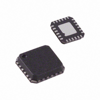
ADN8810ACPZ-REEL7 Analog Devices Inc, ADN8810ACPZ-REEL7 Datasheet - Page 8

ADN8810ACPZ-REEL7
Manufacturer Part Number
ADN8810ACPZ-REEL7
Description
Tunable Laser Controller
Manufacturer
Analog Devices Inc
Datasheet
1.ADN8810ACPZ-REEL7.pdf
(16 pages)
Specifications of ADN8810ACPZ-REEL7
Function
Current Source (12 Bit)
Current - Output
300mA
Operating Temperature
-40°C ~ 85°C
Mounting Type
Surface Mount
Package / Case
24-LFCSP
Lead Free Status / RoHS Status
Lead free / RoHS Compliant
Voltage - Input
-
Accuracy
-
Sensing Method
-
Lead Free Status / RoHS Status
Lead free / RoHS Compliant
ADN8810
ADN8810 TERMINOLOGY
Relative Accuracy
Relative accuracy or integral nonlinearity (INL) is a measure of
the maximum deviation, in least significant bits (LSBs), from an
ideal line passing through the endpoints of the DAC transfer
function. Figure 5 shows a typical INL vs. code plot. The
ADN8810 INL is measured from 2% to 100% of the full-scale
(FS) output.
Differential Nonlinearity
Differential nonlinearity (DNL) is the difference between
the measured change and the ideal 1 LSB change between
any two adjacent codes. A specified differential nonlinearity
of ± 1 LSB maximum ensures monotonicity. The ADN8810
is guaranteed monotonic by design. Figure 6 shows a typical
DNL vs. code plot
Offset Error
Offset error, or zero-code error, is an interpolation of the output
voltage at code 0x000 as predicted by the line formed from the
output voltages at code 0x040 (2% FS) and code 0xFFF (100%
FS). Ideally, the offset error should be 0 V. Offset error occurs
from a combination of the offset voltage of the amplifier and
offset errors in the DAC. It is expressed in LSBs.
Offset Drift
This is a measure of the change in offset error with a change in
temperature. It is expressed in (ppm of full-scale range)/°C.
Gain Error
Gain error is a measure of the span error of the DAC. It is the
deviation in slope of the output transfer characteristic from
ideal. The transfer characteristic is the line formed from the
output voltages at code 0x040 (2% FS) and code 0xFFF (100%
FS). It is expressed as a percent of the full-scale range.
.
Rev. A | Page 8 of 16
Compliance Voltage
The maximum output voltage from the ADN8810 is a function
of output current and supply voltage. Compliance voltage
defines the maximum output voltage at a given current and
supply voltage to guarantee the device operates within its INL,
DNL, and gain error specifications.
Output Current Change vs. Output Voltage Change
This is a measure of the ADN8810 output impedance and is
similar to a load regulation spec in voltage references. For a
given code, the output current changes slightly as output voltage
increases. It is measured as an absolute value in (ppm of full-
scale range)/V.
OFFSET
ERROR
0x040
Figure 4. Output Transfer Function
INTERPOLATED
DAC CODE
(EXAGGERATED)
ACTUAL
IDEAL
0xFFF
GAIN ERROR
PLUS
OFFSET ERROR


