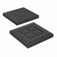
ADSP-21262SBBC-150 Analog Devices Inc, ADSP-21262SBBC-150 Datasheet - Page 20

ADSP-21262SBBC-150
Manufacturer Part Number
ADSP-21262SBBC-150
Description
IC,DSP,32-BIT,CMOS,BGA,136PIN,PLASTIC
Manufacturer
Analog Devices Inc
Series
SHARC®r
Type
Fixed/Floating Pointr
Specifications of ADSP-21262SBBC-150
Interface
DAI, SPI
Clock Rate
150MHz
Non-volatile Memory
ROM (512 kB)
On-chip Ram
256kB
Voltage - I/o
3.30V
Voltage - Core
1.20V
Operating Temperature
-40°C ~ 85°C
Mounting Type
Surface Mount
Package / Case
136-CSPBGA
Device Core Size
32/40Bit
Architecture
Super Harvard
Format
Floating Point
Clock Freq (max)
150MHz
Mips
150
Device Input Clock Speed
150MHz
Ram Size
256KB
Program Memory Size
512KB
Operating Supply Voltage (typ)
1.2/3.3V
Operating Supply Voltage (min)
1.14/3.13V
Operating Supply Voltage (max)
1.26/3.47V
Operating Temp Range
0C to 70C
Operating Temperature Classification
Commercial
Mounting
Surface Mount
Pin Count
136
Package Type
CSPBGA
Lead Free Status / RoHS Status
Contains lead / RoHS non-compliant
Lead Free Status / RoHS Status
Contains lead / RoHS non-compliant
Available stocks
Company
Part Number
Manufacturer
Quantity
Price
Company:
Part Number:
ADSP-21262SBBC-150
Manufacturer:
Analog Devices Inc
Quantity:
10 000
ADSP-21262
Reset
See
Table 11. Reset
1
Interrupts
The timing specification in
FLAG0, FLAG1, and FLAG2 pins when they are configured as
IRQ0, IRQ1, and IRQ2 interrupts. Also applies to DAI_P20–1
pins when configured as interrupts.
Table 12. Interrupts
Core Timer
The timing specification in
FLAG3 when it is configured as the core timer (CTIMER).
Table 13. Core Timer
Parameter
Timing Requirements
t
t
Parameter
Timing Requirement
t
Parameter
Switching Characteristic
t
Applies after the power-up sequence is complete. At power-up, the processor’s internal phase-locked loop requires no more than 100 µs while RESET is low, assuming
WRST
SRST
IPW
WCTIM
stable VDD and CLKIN (not including start-up time of external clock oscillator).
(C TIM E R )
Table 11
F L A G 3
and
Figure
RESET Pulse Width Low
RESET Setup Before CLKIN Low
IRQx Pulse Width
CTIMER Pulse Width
9.
RESET
CLKIN
Table 12
Table 13
and
and
DAI_P20–1
(FLAG2–0)
1
Figure 10
Figure 11
(IRQ2–0)
applies to the
Rev. B | Page 20 of 48 | August 2005
applies to
Figure 11. Core Timer
Figure 10. Interrupts
Figure 9. Reset
t
WRST
Min
4t
8
t
IPW
CK
Min
4 × t
CCLK
t
W C T IM
– 1
Min
2 × t
CCLK
t
SRST
+2
Max
Max
Max
Unit
ns
ns
Unit
ns
Unit
ns


