ADSP-21262SBBC-150 Analog Devices Inc, ADSP-21262SBBC-150 Datasheet - Page 8
ADSP-21262SBBC-150
Manufacturer Part Number
ADSP-21262SBBC-150
Description
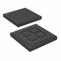
IC,DSP,32-BIT,CMOS,BGA,136PIN,PLASTIC
Manufacturer
Analog Devices Inc
Series
SHARC®r
Type
Fixed/Floating Pointr
Specifications of ADSP-21262SBBC-150
Interface
DAI, SPI
Clock Rate
150MHz
Non-volatile Memory
ROM (512 kB)
On-chip Ram
256kB
Voltage - I/o
3.30V
Voltage - Core
1.20V
Operating Temperature
-40°C ~ 85°C
Mounting Type
Surface Mount
Package / Case
136-CSPBGA
Device Core Size
32/40Bit
Architecture
Super Harvard
Format
Floating Point
Clock Freq (max)
150MHz
Mips
150
Device Input Clock Speed
150MHz
Ram Size
256KB
Program Memory Size
512KB
Operating Supply Voltage (typ)
1.2/3.3V
Operating Supply Voltage (min)
1.14/3.13V
Operating Supply Voltage (max)
1.26/3.47V
Operating Temp Range
0C to 70C
Operating Temperature Classification
Commercial
Mounting
Surface Mount
Pin Count
136
Package Type
CSPBGA
Lead Free Status / RoHS Status
Contains lead / RoHS non-compliant
Lead Free Status / RoHS Status
Contains lead / RoHS non-compliant
Available stocks
Company
Part Number
Manufacturer
Quantity
Price
Company:

Part Number:
ADSP-21262SBBC-150
Manufacturer:
Analog Devices Inc
Quantity:
10 000


ADSP-21262
interface consisting of two data pins, one device select pin, and
one clock pin. It is a full-duplex synchronous serial interface,
supporting both master and slave modes. The SPI port can
operate in a multimaster environment by interfacing with up to
four other SPI-compatible devices, either acting as a master or
slave device. The ADSP-21262 SPI-compatible peripheral
implementation also features programmable baud rates up to
37.5 MHz, clock phases, and polarities. The ADSP-21262 SPI-
compatible port uses open drain drivers to support a multimas-
ter configuration and to avoid data contention.
Parallel Port
The parallel port provides interfaces to SRAM and peripheral
devices. The multiplexed address and data pins (AD15–0) can
access 8-bit devices with up to 24 bits of address, or 16-bit
devices with up to 16 bits of address. In either mode, 8- or 16-
bit, the maximum data transfer rate is one-third the core clock
speed. As an example, a clock rate of 200 MHz is equivalent to
66M byte/sec, and a clock rate of 150 MHz is equivalent to
50M byte/sec.
DMA transfers are used to move data to and from internal
memory. Access to the core is also facilitated through the paral-
lel port register read/write functions. The RD, WR, and ALE
(address latch enable) pins are the control pins for the
parallel port.
Timers
The ADSP-21262 has a total of four timers: a core timer able to
generate periodic software interrupts, and three general-pur-
pose timers that can generate periodic interrupts and be
independently set to operate in one of three modes:
The core timer can be configured to use FLAG3 as a timer
expired output signal, and each general-purpose timer has one
bidirectional pin and four registers that implement its mode of
operation: a 6-bit configuration register, a 32-bit count register,
a 32-bit period register, and a 32-bit pulse width register. A sin-
gle control and status register enables or disables all three
general-purpose timers independently.
Program Booting
The internal memory of the ADSP-21262 boots at system
power-up from an 8-bit EPROM via the parallel port, an SPI
master, an SPI slave, or an internal boot. Booting is determined
by the boot configuration (BOOTCFG1–0) pins. Selection of the
boot source is controlled via the SPI as either a master or slave
device, or it can immediately begin executing from ROM.
Phase-Locked Loop
The ADSP-21262 uses an on-chip phase-locked loop (PLL) to
generate the internal clock for the core. On power-up, the
CLKCFG1-0 pins are used to select ratios of 16:1, 8:1, and 3:1.
After booting, numerous other ratios can be selected via soft-
• Pulse waveform generation mode
• Pulse width count/capture mode
• External event watchdog mode
Rev. B | Page 8 of 48 | August 2005
ware control. The ratios are made up of software configurable
numerator values from 1 to 32 and software configurable divi-
sor values of 1, 2, 4, 8, and 16.
Power Supplies
The ADSP-21262 has separate power supply connections for the
internal (V
power supplies. The internal and analog supplies must meet the
1.2 V requirement. The external supply must meet the 3.3 V
requirement. All external supply pins must be connected to the
same power supply.
Note that the analog supply pin (A
internal clock generator PLL. To produce a stable clock, it is rec-
ommended that PCB designs use an external filter circuit for the
A
A
mended ferrite chip is the muRata BLM18AG102SN1D). To
reduce noise coupling, the PCB should use a parallel pair of
power and ground planes for V
to connect the bypass capacitors to the analog power (A
ground (A
in
ground plane on the board—the A
directly to digital ground (GND) at the chip.
TARGET BOARD JTAG EMULATOR CONNECTOR
Analog Devices DSP Tools product line of JTAG emulators uses
the IEEE 1149.1 JTAG test access port of the ADSP-21262 pro-
cessor to monitor and control the target board processor during
emulation. Analog Devices DSP Tools product line of JTAG
emulators provides emulation at full processor speed, allowing
inspection and modification of memory, registers, and proces-
sor stacks. The processor’s JTAG interface ensures that the
emulator will not affect target system loading or timing.
For complete information on Analog Devices’ SHARC DSP
Tools product line of JTAG emulator operation, see the appro-
priate emulator hardware user’s guide.
VDD
VDD
V DDINT
Figure 4
/A
pin. Place the filter components as close as possible to the
VSS
HI Z FERRITE
VSS
pins. For an example circuit, see
BEAD CHIP
DDINT
are inputs to the processor and not the analog
) pins. Note that the A
), external (V
Figure 4. Analog Power Filter Circuit
CLOSE TO A VDD AND A VSS PINS
100nF
LOCATE ALL COMPONENTS
DDEXT
10nF
DDINT
), and analog (A
VSS
VDD
VDD
and GND. Use wide traces
pin should connect
) powers the processor’s
1nF
and A
Figure
VSS
pins specified
ADSP-21262
A VDD
A VSS
VDD
4. (A recom-
/A
VDD
VSS
) and
)
Related parts for ADSP-21262SBBC-150
Image
Part Number
Description
Manufacturer
Datasheet
Request
R

Part Number:
Description:
±1.7g Dual-Axis IMEMS Accelerometer Evaluation Board
Manufacturer:
Analog Devices Inc
Datasheet:

Part Number:
Description:
Inertial Sensor Evaluation System
Manufacturer:
Analog Devices Inc
Datasheet:
Part Number:
Description:
Manufacturer:
Analog Devices Inc
Datasheet:
Part Number:
Description:
Manufacturer:
Analog Devices Inc
Datasheet:
Part Number:
Description:
Manufacturer:
Analog Devices Inc
Datasheet:
Part Number:
Description:
Manufacturer:
Analog Devices Inc
Datasheet:
Part Number:
Description:
Manufacturer:
Analog Devices Inc
Datasheet:
Part Number:
Description:
Manufacturer:
Analog Devices Inc
Datasheet:
Part Number:
Description:
Manufacturer:
Analog Devices Inc
Datasheet:
Part Number:
Description:
Manufacturer:
Analog Devices Inc
Datasheet:
Part Number:
Description:
Manufacturer:
Analog Devices Inc
Datasheet:
Part Number:
Description:
Manufacturer:
Analog Devices Inc
Datasheet:
Part Number:
Description:
Manufacturer:
Analog Devices Inc
Datasheet: