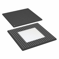
ADSP-21368BBPZ-2A Analog Devices Inc, ADSP-21368BBPZ-2A Datasheet - Page 21

ADSP-21368BBPZ-2A
Manufacturer Part Number
ADSP-21368BBPZ-2A
Description
IC,DSP,32-BIT,CMOS,BGA,256PIN,PLASTIC
Manufacturer
Analog Devices Inc
Series
SHARC®r
Type
Floating Pointr
Datasheet
1.ADSP-21369KBPZ-2A.pdf
(60 pages)
Specifications of ADSP-21368BBPZ-2A
Interface
DAI, DPI
Clock Rate
333MHz
Non-volatile Memory
ROM (768 kB)
On-chip Ram
256kB
Voltage - I/o
3.30V
Voltage - Core
1.20V
Operating Temperature
-40°C ~ 85°C
Mounting Type
Surface Mount
Package / Case
256-BGA Exposed Pad, 256-eBGA, 256-HBGA
Device Core Size
32/40Bit
Architecture
Super Harvard
Format
Floating Point
Clock Freq (max)
333MHz
Mips
333
Device Input Clock Speed
333MHz
Ram Size
256KB
Program Memory Size
768KB
Operating Supply Voltage (typ)
1.2/3.3V
Operating Supply Voltage (min)
1.14/3.13V
Operating Supply Voltage (max)
1.26/3.47V
Operating Temp Range
-40C to 85C
Operating Temperature Classification
Industrial
Mounting
Surface Mount
Pin Count
256
Package Type
SBGA
Lead Free Status / RoHS Status
Lead free / RoHS Compliant
Lead Free Status / RoHS Status
Lead free / RoHS Compliant
Available stocks
Company
Part Number
Manufacturer
Quantity
Price
Company:
Part Number:
ADSP-21368BBPZ-2A
Manufacturer:
Analog Devices Inc
Quantity:
10 000
Clock Input
Table 13. Clock Input
1
2
3
4
5
6
7
8
9
10
Parameter
Timing Requirements
t
t
t
t
t
f
t
Applies to all 400 MHz models. See
Applies to all 366 MHz models. See
Applies to all 350 MHz models. See
Applies to all 333 MHz models. See
Applies to all 266 MHz models. See
Applies only for CLK_CFG1–0 = 00 and default values for PLL control bits in PMCTL.
Any changes to PLL control bits in the PMCTL register must meet core clock timing specification t
See
Actual input jitter should be combined with ac specifications for accurate timing analysis.
Jitter specification is maximum peak-to-peak time interval error (TIE) jitter.
VCO
CK
CKL
CKH
CKRF
CCLK
CKJ
9, 10
8
7
Figure 5 on Page 19
CLKIN Period
CLKIN Width Low
CLKIN Width High
CLKIN Rise/Fall (0.4 V to 2.0 V)
CCLK Period
VCO Frequency
CLKIN Jitter Tolerance
CLKIN
for VCO diagram.
t
CKH
Ordering Guide on Page
Ordering Guide on Page
Ordering Guide on Page
Ordering Guide on Page
Ordering Guide on Page
400 MHz
Min
15
7.5
7.5
2.5
100
–250
6
1
1
6
t
CK
t
CKL
58.
58.
58.
58.
58.
Max
100
45
45
3
10
800
+250
1
Figure 7. Clock Input
Rev. E | Page 21 of 60 | July 2009
366 MHz
Min
16.39
8.1
8.1
2.73
100
–250
1
1
6
6
Max
100
45
45
3
10
800
+250
2
ADSP-21367/ADSP-21368/ADSP-21369
350 MHz
Min
17.14
8.5
8.5
2.85
100
–250
CCLK
1
1
6
.
6
t
CKJ
Max
100
45
45
3
10
800
+250
3
333 MHz
Min
18
9
9
3.0
100
–250
1
1
6
6
Max
100
45
45
3
10
800
+250
4
266 MHz
Min
22.5
11.25
11.25
3.75
100
–250
6
6
1
1
Max
100
45
45
3
10
600
+250
5
Unit
ns
ns
ns
ns
ns
MHz
ps


