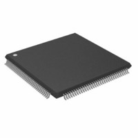
ADSP-2191MBSTZ-140 Analog Devices Inc, ADSP-2191MBSTZ-140 Datasheet - Page 17

ADSP-2191MBSTZ-140
Manufacturer Part Number
ADSP-2191MBSTZ-140
Description
IC,DSP,16-BIT,CMOS,QFP,144PIN,PLASTIC
Manufacturer
Analog Devices Inc
Series
ADSP-21xxr
Type
Fixed Pointr
Specifications of ADSP-2191MBSTZ-140
Interface
Host Interface, SPI, SSP, UART
Clock Rate
140MHz
Non-volatile Memory
External
On-chip Ram
160kB
Voltage - I/o
3.00V, 3.30V
Voltage - Core
2.50V
Operating Temperature
-40°C ~ 85°C
Mounting Type
Surface Mount
Package / Case
144-LQFP
Device Core Size
16b
Clock Freq (max)
140MHz
Mips
140
Device Input Clock Speed
140MHz
Ram Size
160KB
Operating Supply Voltage (typ)
2.5/3.3V
Operating Supply Voltage (min)
2.37/2.97V
Operating Supply Voltage (max)
2.63/3.6V
Operating Temp Range
-40C to 85C
Operating Temperature Classification
Industrial
Mounting
Surface Mount
Pin Count
144
Package Type
LQFP
Lead Free Status / RoHS Status
Lead free / RoHS Compliant
Lead Free Status / RoHS Status
Lead free / RoHS Compliant
Other names
ADSP-2191MBSTZ140
Available stocks
Company
Part Number
Manufacturer
Quantity
Price
Company:
Part Number:
ADSP-2191MBSTZ-140
Manufacturer:
MAXIM
Quantity:
101
Company:
Part Number:
ADSP-2191MBSTZ-140
Manufacturer:
Analog Devices Inc
Quantity:
10 000
Table 7. Pin Function Descriptions (continued)
REV. A
Pin
TMR2–0
RXD
TXD
RESET
TCK
TMS
TDI
TDO
TRST
EMU
V
V
GND
NC
DDINT
DDEXT
Type
I/O/T
I
O
I
I
I
I
O
I
O
P
P
G
Function
Timer Output or Capture
UART Serial Receive Data
UART Serial Transmit Data
Processor Reset. Resets the ADSP-2191M to a known state and begins execution at the
program memory location specified by the hardware reset vector address. The RESET input
must be asserted (low) at powerup. The RESET pin has an 85 kΩ internal pull-up resistor.
Test Clock (JTAG). Provides a clock for JTAG boundary scan. The TCK pin has an 85 kΩ
internal pull-up resistor.
Test Mode Select (JTAG). Used to control the test state machine. The TMS pin has an 85 kΩ
internal pull-up resistor.
Test Data Input (JTAG). Provides serial data for the boundary scan logic. The TDI pin has a
85 kΩ internal pull-up resistor.
Test Data Output (JTAG). Serial scan output of the boundary scan path.
Test Reset (JTAG). Resets the test state machine. TRST must be asserted (pulsed low) after
powerup or held low for proper operation of the ADSP-2191M. The TRST pin has a 65 kΩ
internal pull-down resistor.
Emulation Status (JTAG). Must be connected to the ADSP-2191M emulator target board
connector only.
Core Power Supply. Nominally 2.5 V dc and supplies the DSP’s core processor. (four pins)
I/O Power Supply. Nominally 3.3 V dc. (nine pins)
Power Supply Return. (twelve pins)
Do Not Connect. Reserved pins that must be left open and unconnected.
–17–
ADSP-2191M


