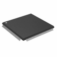
ADSP-2191MBSTZ-140 Analog Devices Inc, ADSP-2191MBSTZ-140 Datasheet - Page 3

ADSP-2191MBSTZ-140
Manufacturer Part Number
ADSP-2191MBSTZ-140
Description
IC,DSP,16-BIT,CMOS,QFP,144PIN,PLASTIC
Manufacturer
Analog Devices Inc
Series
ADSP-21xxr
Type
Fixed Pointr
Specifications of ADSP-2191MBSTZ-140
Interface
Host Interface, SPI, SSP, UART
Clock Rate
140MHz
Non-volatile Memory
External
On-chip Ram
160kB
Voltage - I/o
3.00V, 3.30V
Voltage - Core
2.50V
Operating Temperature
-40°C ~ 85°C
Mounting Type
Surface Mount
Package / Case
144-LQFP
Device Core Size
16b
Clock Freq (max)
140MHz
Mips
140
Device Input Clock Speed
140MHz
Ram Size
160KB
Operating Supply Voltage (typ)
2.5/3.3V
Operating Supply Voltage (min)
2.37/2.97V
Operating Supply Voltage (max)
2.63/3.6V
Operating Temp Range
-40C to 85C
Operating Temperature Classification
Industrial
Mounting
Surface Mount
Pin Count
144
Package Type
LQFP
Lead Free Status / RoHS Status
Lead free / RoHS Compliant
Lead Free Status / RoHS Status
Lead free / RoHS Compliant
Other names
ADSP-2191MBSTZ140
Available stocks
Company
Part Number
Manufacturer
Quantity
Price
Company:
Part Number:
ADSP-2191MBSTZ-140
Manufacturer:
MAXIM
Quantity:
101
Company:
Part Number:
ADSP-2191MBSTZ-140
Manufacturer:
Analog Devices Inc
Quantity:
10 000
GENERAL DESCRIPTION
The ADSP-2191M DSP is a single-chip microcomputer
optimized for digital signal processing (DSP) and other high
speed numeric processing applications.
The ADSP-2191M combines the ADSP-219x family base
architecture (three computational units, two data address gener-
ators, and a program sequencer) with three serial ports, two
SPI-compatible ports, one UART port, a DMA controller, three
programmable timers, general-purpose Programmable Flag
pins, extensive interrupt capabilities, and on-chip program and
data memory spaces.
The ADSP-2191M architecture is code-compatible with DSPs
of the ADSP-218x family. Although the architectures are
compatible, the ADSP-2191M architecture has a number of
enhancements over the ADSP-218x architecture. The enhance-
ments to computational units, data address generators, and
program sequencer make the ADSP-2191M more flexible and
even easier to program.
Indirect addressing options provide addressing flexibility—
premodify with no update, pre- and post-modify by an immediate
8-bit, two’s-complement value and base address registers for
easier implementation of circular buffering.
The ADSP-2191M integrates 64K words of on-chip memory
configured as 32K words (24-bit) of program RAM, and
32K words (16-bit) of data RAM. Power-down circuitry is also
provided to reduce power consumption. The ADSP-2191M is
available in 144-lead LQFP and 144-ball mini-BGA packages.
Fabricated in a high speed, low power, CMOS process, the
ADSP-2191M operates with a 6.25 ns instruction cycle time
(160 MIPS). All instructions, except single-word instructions,
execute in one processor.
The ADSP-2191M’s flexible architecture and comprehensive
instruction set support multiple operations in parallel. For
example, in one processor cycle, the ADSP-2191M can:
• Generate an address for the next instruction fetch
• Fetch the next instruction
• Perform one or two data moves
• Update one or two data address pointers
• Perform a computational operation
These operations take place while the processor continues to:
• Receive and transmit data through two serial ports
• Receive and/or transmit data from a Host
• Receive or transmit data through the UART
• Receive or transmit data over two SPI ports
• Access external memory through the external memory
• Decrement the timers
DSP Core Architecture
The ADSP-2191M instruction set provides flexible data moves
and multifunction (one or two data moves with a computation)
instructions. Every single-word instruction can be executed in a
single processor cycle. The ADSP-2191M assembly language
REV. A
interface
–3–
uses an algebraic syntax for ease of coding and readability. A
comprehensive set of development tools supports program
development.
The functional block diagram
of the ADSP-219x core. It contains three independent compu-
tational units: the ALU, the multiplier/accumulator (MAC), and
the shifter. The computational units process 16-bit data from the
register file and have provisions to support multiprecision com-
putations. The ALU performs a standard set of arithmetic and
logic operations; division primitives are also supported. The
MAC performs single-cycle multiply, multiply/add, and multi-
ply/subtract operations. The MAC has two 40-bit accumulators,
which help with overflow. The shifter performs logical and arith-
metic shifts, normalization, denormalization, and derive
exponent operations. The shifter can be used to efficiently
implement numeric format control, including multiword and
block floating-point representations.
Register-usage rules influence placement of input and results
within the computational units. For most operations, the com-
putational units’ data registers act as a data register file,
permitting any input or result register to provide input to any unit
for a computation. For feedback operations, the computational
units let the output (result) of any unit be input to any unit on
the next cycle. For conditional or multifunction instructions,
there are restrictions on which data registers may provide inputs
or receive results from each computational unit. For more infor-
mation, see the ADSP-219x DSP Instruction Set Reference.
A powerful program sequencer controls the flow of instruction
execution. The sequencer supports conditional jumps, subrou-
tine calls, and low interrupt overhead. With internal loop
counters and loop stacks, the ADSP-2191M executes looped
code with zero overhead; no explicit jump instructions are
required to maintain loops.
Two data address generators (DAGs) provide addresses for
simultaneous dual operand fetches (from data memory and
program memory). Each DAG maintains and updates four
16-bit address pointers. Whenever the pointer is used to access
data (indirect addressing), it is pre- or post-modified by the value
of one of four possible modify registers. A length value and base
address may be associated with each pointer to implement
automatic modulo addressing for circular buffers. Page registers
in the DAGs allow circular addressing within 64K-word bound-
aries of each of the 256 memory pages, but these buffers may not
cross page boundaries. Secondary registers duplicate all the
primary registers in the DAGs; switching between primary and
secondary registers provides a fast context switch.
Efficient data transfer in the core is achieved with the use of
internal buses:
• Program Memory Address (PMA) Bus
• Program Memory Data (PMD) Bus
• Data Memory Address (DMA) Bus
• Data Memory Data (DMD) Bus
• DMA Address Bus
• DMA Data Bus
on Page 1
ADSP-2191M
shows the architecture


