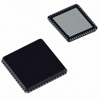
ADUC841BCPZ8-5 Analog Devices Inc, ADUC841BCPZ8-5 Datasheet - Page 37

ADUC841BCPZ8-5
Manufacturer Part Number
ADUC841BCPZ8-5
Description
IC,Data Acquisition CODEC,2-CHANNEL,LLCC,56PIN,PLASTIC
Manufacturer
Analog Devices Inc
Series
MicroConverter® ADuC8xxr
Datasheet
1.EVAL-ADUC842QS.pdf
(88 pages)
Specifications of ADUC841BCPZ8-5
Core Processor
8052
Core Size
8-Bit
Speed
20MHz
Connectivity
I²C, SPI, UART/USART
Peripherals
DMA, PSM, PWM, Temp Sensor, WDT
Number Of I /o
32
Program Memory Size
8KB (8K x 8)
Program Memory Type
FLASH
Ram Size
2.25K x 8
Voltage - Supply (vcc/vdd)
4.75 V ~ 5.25 V
Data Converters
A/D 8x12b, D/A 2x12b
Oscillator Type
Internal
Operating Temperature
-40°C ~ 85°C
Package / Case
56-LFCSP
Lead Free Status / RoHS Status
Lead free / RoHS Compliant
For Use With
EVAL-ADUC841QSZ - KIT DEV FOR ADUC841 QUICK START
Eeprom Size
-
Lead Free Status / RoHS Status
Lead free / RoHS Compliant
Available stocks
Company
Part Number
Manufacturer
Quantity
Price
Part Number:
ADUC841BCPZ8-5
Manufacturer:
ADI/亚德诺
Quantity:
20 000
CFG841
SFR Address
Power-On Default
Bit Addressable
Table 14. CFG841 SFR Bit Designations
Bit No.
7
6
5
4
3
2
1
0
1
these bits so all instructions to the CFG841 register should use the ORL, XRL, or ANL instructions. Value of 10H is for 11.0592 MHz crystal.
Note that the Flash/EE controller bits EPM2, EPM1, EPM0 are set to their correct values depending on the crystal frequency at power-up. The user should not modify
Name
EXSP
PWPO
DBUF
EPM2
EPM1
EPM0
MSPI
XRAMEN
Description
Extended SP Enable.
When set to 1 by the user, the stack rolls over from SPH/SP = 00FFH to 0100H.
When set to 0 by the user, the stack rolls over from SP = FFH to SP = 00H.
PWM Pin Out Selection.
Set to 1 by the user to select P3.4 and P3.3 as the PWM output pins.
Set to 0 by the user to select P2.6 and P2.7 as the PWM output pins.
DAC Output Buffer.
Set to 1 by the user to bypass the DAC output buffer.
Set to 0 by the user to enable the DAC output buffer.
Flash/EE Controller and PWM Clock Frequency Configuration Bits.
Frequency should be configured such that F
EPM2
0
0
0
0
1
1
Set to 1 by the user to move the SPI functionality of MISO, MOSI, and SCLOCK to P3.3, P3.4, and P3.5,
respectively.
Set to 0 by the user to leave the SPI functionality as usual on MISO, MOSI, and SCLOCK pins.
XRAM Enable Bit.
When set to 1 by the user, the internal XRAM is mapped into the lower two kBytes of the external address
space.
When set to 0 by the user, the internal XRAM is not accessible, and the external data memory is mapped into
the lower two kBytes of external data memory.
ADuC841 Config SFR
AFH
10H
No
0
EPM1
0
1
1
0
0
1
0
0
EPM0
1
0
1
1
32
Divide Factor
64
128
256
512
1024
Rev. 0 | Page 37 of 88
OSC
/Divide Factor = 32 kHz + 50%.
ADuC841/ADuC842/ADuC843


