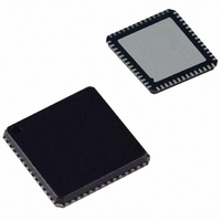
ADUC841BCPZ8-5 Analog Devices Inc, ADUC841BCPZ8-5 Datasheet - Page 46

ADUC841BCPZ8-5
Manufacturer Part Number
ADUC841BCPZ8-5
Description
IC,Data Acquisition CODEC,2-CHANNEL,LLCC,56PIN,PLASTIC
Manufacturer
Analog Devices Inc
Series
MicroConverter® ADuC8xxr
Datasheet
1.EVAL-ADUC842QS.pdf
(88 pages)
Specifications of ADUC841BCPZ8-5
Core Processor
8052
Core Size
8-Bit
Speed
20MHz
Connectivity
I²C, SPI, UART/USART
Peripherals
DMA, PSM, PWM, Temp Sensor, WDT
Number Of I /o
32
Program Memory Size
8KB (8K x 8)
Program Memory Type
FLASH
Ram Size
2.25K x 8
Voltage - Supply (vcc/vdd)
4.75 V ~ 5.25 V
Data Converters
A/D 8x12b, D/A 2x12b
Oscillator Type
Internal
Operating Temperature
-40°C ~ 85°C
Package / Case
56-LFCSP
Lead Free Status / RoHS Status
Lead free / RoHS Compliant
For Use With
EVAL-ADUC841QSZ - KIT DEV FOR ADUC841 QUICK START
Eeprom Size
-
Lead Free Status / RoHS Status
Lead free / RoHS Compliant
Available stocks
Company
Part Number
Manufacturer
Quantity
Price
Part Number:
ADUC841BCPZ8-5
Manufacturer:
ADI/亚德诺
Quantity:
20 000
ADuC841/ADuC842/ADuC843
SPICON SPI Control Register
SFR Address
Power-On Default
Bit Addressable
Table 18. SPICON SFR Bit Designations
Bit No.
7
6
5
4
3
2
1
0
SPIDAT
Function
SFR Address
Power-On Default
Bit Addressable
1
The CPOL and CPHA bits should both contain the same values for master and slave devices.
Name
ISPI
WCOL
SPE
SPIM
CPOL
CPHA
SPR1
SPR0
1
1
Description
SPI Interrupt Bit.
Set by the MicroConverter at the end of each SPI transfer.
Cleared directly by user code or indirectly by reading the SPIDAT SFR.
Write Collision Error Bit.
Set by the MicroConverter if SPIDAT is written to while an SPI transfer is in progress.
Cleared by user code.
SPI Interface Enable Bit.
Set by the user to enable the SPI interface.
Cleared by the user to enable the I
CFG841/CFG842. In this case, the I
SPI Master/Slave Mode Select Bit.
Set by the user to enable master mode operation (SCLOCK is an output).
Cleared by the user to enable slave mode operation (SCLOCK is an input).
Clock Polarity Select Bit.
Set by the user if SCLOCK idles high.
Cleared by the user if SCLOCK idles low.
Clock Phase Select Bit.
Set by the user if leading SCLOCK edge is to transmit data.
Cleared by the user if trailing SCLOCK edge is to transmit data.
SPI Bit Rate Select Bits.
These bits select the SCLOCK rate (bit rate) in master mode as follows:
SPR1
0
0
1
1
In SPI slave mode, i.e., SPIM = 0, the logic level on the external SS pin can be read via the SPR0 bit.
F8H
04H
Yes
SPI Data Register
SPIDAT SFR is written by the user to transmit data over the SPI interface or read by user code to
read data just received by the SPI interface.
F7H
00H
No
SPR0
0
1
0
1
Selected Bit Rate
f
f
f
f
OSC
OSC
OSC
OSC
/2
/4
/8
/16
2
2
C interface is automatically enabled.
C pins, this is not requiredto enable the I
Rev. 0 | Page 46 of 88
2
C interface if the MSPI bit is set in


