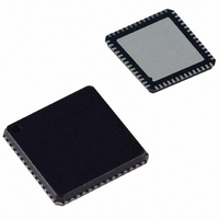
ADUC841BCPZ8-5 Analog Devices Inc, ADUC841BCPZ8-5 Datasheet - Page 61

ADUC841BCPZ8-5
Manufacturer Part Number
ADUC841BCPZ8-5
Description
IC,Data Acquisition CODEC,2-CHANNEL,LLCC,56PIN,PLASTIC
Manufacturer
Analog Devices Inc
Series
MicroConverter® ADuC8xxr
Datasheet
1.EVAL-ADUC842QS.pdf
(88 pages)
Specifications of ADUC841BCPZ8-5
Core Processor
8052
Core Size
8-Bit
Speed
20MHz
Connectivity
I²C, SPI, UART/USART
Peripherals
DMA, PSM, PWM, Temp Sensor, WDT
Number Of I /o
32
Program Memory Size
8KB (8K x 8)
Program Memory Type
FLASH
Ram Size
2.25K x 8
Voltage - Supply (vcc/vdd)
4.75 V ~ 5.25 V
Data Converters
A/D 8x12b, D/A 2x12b
Oscillator Type
Internal
Operating Temperature
-40°C ~ 85°C
Package / Case
56-LFCSP
Lead Free Status / RoHS Status
Lead free / RoHS Compliant
For Use With
EVAL-ADUC841QSZ - KIT DEV FOR ADUC841 QUICK START
Eeprom Size
-
Lead Free Status / RoHS Status
Lead free / RoHS Compliant
Available stocks
Company
Part Number
Manufacturer
Quantity
Price
Part Number:
ADUC841BCPZ8-5
Manufacturer:
ADI/亚德诺
Quantity:
20 000
TCON
SFR Address
Power-On Default
Bit Addressable
Table 29. TCON SFR Bit Designations
Bit No.
7
6
5
4
3
2
1
0
1
Timer/Counter 0 and 1 Data Registers
Each timer consists of two 8-bit registers. These can be used as
independent registers or combined into a single 16-bit register
depending on the timer mode configuration.
These bits are not used in the control of Timer/Counter 0 and 1, but are used instead in the control and monitoring of the external INT0 and INT1 interrupt pins.
Name
TF1
TR1
TF0
TR0
IE1
IT1
IE0
IT0
1
1
1
1
Description
Timer 1 Overflow Flag.
Set by hardware on a Timer/Counter 1 overflow.
Cleared by hardware when the program counter (PC) vectors to the interrupt service routine.
Timer 1 Run Control Bit.
Set by the user to turn on Timer/Counter 1.
Cleared by the user to turn off Timer/Counter 1.
Timer 0 Overflow Flag.
Set by hardware on a Timer/Counter 0 overflow.
Cleared by hardware when the PC vectors to the interrupt service routine.
Timer 0 Run Control Bit.
Set by the user to turn on Timer/Counter 0.
Cleared by the user to turn off Timer/Counter 0.
External Interrupt 1 (INT1) Flag.
Set by hardware by a falling edge or by a zero level being applied to the external interrupt pin, INT1, depending on
the state of Bit IT1.
Cleared by hardware when the PC vectors to the interrupt service routine only if the interrupt was transition-
activated. If level-activated, the external requesting source controls the request flag, rather than the on-chip
hardware.
External Interrupt 1 (IE1) Trigger Type.
Set by software to specify edge-sensitive detection, i.e., 1-to-0 transition.
Cleared by software to specify level-sensitive detection, i.e., zero level.
External Interrupt 0 (INT0) Flag.
Set by hardware by a falling edge or by a zero level being applied to external interrupt pin INT0, depending on the
state of Bit IT0.
Cleared by hardware when the PC vectors to the interrupt service routine only if the interrupt was transition-
activated. If level-activated, the external requesting source controls the request flag, rather than the on-chip
hardware.
External Interrupt 0 (IE0) Trigger Type.
Set by software to specify edge-sensitive detection, i.e.,1-to-0 transition.
Cleared by software to specify level-sensitive detection, i.e., zero level.
Timer/Counter 0 and 1
Control Register
88H
00H
Yes
Rev. 0 | Page 61 of 88
TH0 and TL0
Timer 0 high byte and low byte.
SFR Address = 8CH 8AH, respectively.
TH1 and TL1
Timer 1 high byte and low byte.
SFR Address = 8DH, 8BH, respectively.
ADuC841/ADuC842/ADuC843


