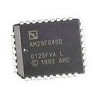
AM29F010B-90JC Spansion Inc., AM29F010B-90JC Datasheet - Page 18

AM29F010B-90JC
Manufacturer Part Number
AM29F010B-90JC
Description
Flash Memory IC
Manufacturer
Spansion Inc.
Datasheet
1.AM29F010B-90JC.pdf
(33 pages)
Specifications of AM29F010B-90JC
Memory Size
1Mbit
Memory Configuration
128K X 8
Ic Interface Type
Parallel
Access Time
90ns
Memory Case Style
PLCC
No. Of Pins
32
Peak Reflow Compatible (260 C)
No
Supply Voltage Max
5.5V
Lead Free Status / RoHS Status
Contains lead / RoHS non-compliant
Available stocks
Company
Part Number
Manufacturer
Quantity
Price
Part Number:
AM29F010B-90JC
Manufacturer:
AMD
Quantity:
20 000
The DQ5 failure condition may appear if the system
tries to program a “1” to a location that is previously pro-
grammed to “0.” Only an erase operation can change
a “0” back to a “1.” Under this condition, the device
halts the operation, and when the operation has ex-
ceeded the timing limits, DQ5 produces a “1.”
Under both these conditions, the system must issue the
reset command to return the device to reading array
data.
DQ3: Sector Erase Timer
After writing a sector erase command sequence, the
system may read DQ3 to determine whether or not an
erase operation has begun. (The sector erase timer
does not apply to the chip erase command.) If addi-
tional sectors are selected for erasure, the entire time-
out also applies after each additional sector erase com-
mand. When the time-out is complete, DQ3 switches
from “0” to “1.” The system may ignore DQ3 if the sys-
Notes:
1. DQ7 requires a valid address when reading status information. Refer to the appropriate subsection for further details.
2. DQ5 switches to ‘1’ when an Embedded Program or Embedded Erase operation has exceeded the maximum timing limits.
16
Standard
Mode
Erase
Suspend
Mode
See “DQ5: Exceeded Timing Limits” for more information.
Embedded Program Algorithm
Embedded Erase Algorithm
Reading within Erase Suspended Sector
Reading within Non-Erase Suspended Sector
Operation
Table 5. Write Operation Status
D A T A
Am29F010B
S H E E T
tem can guarantee that the time between additional
sector erase commands will always be less than 50 μs.
See also the “Sector Erase Command Sequence”
section.
After the sector erase command sequence is written,
the system should read the status on DQ7 (Data# Poll-
ing) or DQ6 (Toggle Bit I) to ensure the device has
accepted the command sequence, and then read DQ3.
If DQ3 is “1”, the internally controlled erase cycle has
begun; all further commands are ignored until the
erase operation is complete. If DQ3 is “0”, the device
will accept additional sector erase commands. To en-
sure the command has been accepted, the system
software should check the status of DQ3 prior to and
following each subsequent sector erase command. If
DQ3 is high on the second status check, the last com-
mand might not have been accepted. Table 5 shows
the outputs for DQ3.
(Note 1)
DQ7#
DQ7
Data
0
1
No toggle
Toggle
Toggle
DQ6
Data
Am29F010B_00_C7 October 31, 2006
(Note 2)
DQ5
Data
0
0
0
DQ3
Data
N/A
N/A
1


