CY62136EV30LL-45BVXIT Cypress Semiconductor Corp, CY62136EV30LL-45BVXIT Datasheet
CY62136EV30LL-45BVXIT
Specifications of CY62136EV30LL-45BVXIT
Available stocks


Related parts for CY62136EV30LL-45BVXIT

CY62136EV30LL-45BVXIT Summary of contents
Page 1
... Note 1. For best practice recommendations, refer to the Cypress application note “SRAM System Design Guidelines” on http://www.cypress.com. Cypress Semiconductor Corporation Document #: 38-05569 Rev. *D 2-Mbit (128K x 16) Static RAM Functional Description The CY62136EV30 organized as 128 K words by 16 bits. This device features advanced circuit design to provide ultra low active current. This is ideal for providing More Battery Life™ ...
Page 2
Contents Pin Configuration .............................................................. 3 Product Portfolio ............................................................... 3 Maximum Ratings ............................................................. 4 Operating Range ............................................................... 4 Electrical Characteristics.................................................. 4 Capacitance ...................................................................... 4 Thermal Resistance .......................................................... 5 Data Retention Characteristics ....................................... 5 Data Retention Waveform ................................................ 5 Switching Characteristics................................................. 6 ...
Page 3
... Product V Range (V) CC Min Typ CY62136EV30LL 2.2 3.0 Notes 2. NC pins are not connected on the die. 3. Pins D3, H1, G2, H6 and H3 in the VFBGA package are address expansion pins for 4 Mb, 8 Mb, 16 Mb, and 32 Mb and 64 Mb respectively 4. Typical values are included for reference only and are not guaranteed or tested. Typical values are measured at V Document #: 38-05569 Rev ...
Page 4
... Tested initially and after any design or process changes that may affect these parameters. Document #: 38-05569 Rev input voltage Output current into outputs (LOW) ............................. 20 mA Static discharge voltage ......................................... > 2001 V (per MIL-STD-883, Method 3015) Latch up current ..................................................... > 200 mA Operating Range Device + 0 MAX CY62136EV30LL Industrial + 0 MAX Test Conditions = –0 2. –1 2. ...
Page 5
Thermal Resistance Parameter [11] Description Thermal resistance JA (junction to ambient) Thermal resistance JC (junction to case OUTPUT 30 pF INCLUDING JIG AND SCOPE Parameters Data Retention Characteristics (Over ...
Page 6
Switching Characteristics Over the Operating Range Parameter [16, 17] Read Cycle t Read cycle time RC t Address to data valid AA t Data hold from address change OHA t CE LOW to data valid ACE t OE LOW to ...
Page 7
Switching Waveforms Figure 2. Read Cycle 1: Address Transition Controlled ADDRESS DATA OUT PREVIOUS DATA VALID Figure 3. Read Cycle No Controlled ADDRESS CE t ACE OE BHE/BLE t LZOE t DBE t LZBE HIGH IMPEDANCE DATA ...
Page 8
Switching Waveforms (continued) Figure 4. Write Cycle No Controlled ADDRESS BHE/BLE OE 27 DATA I/O NOTE t HZOE Figure 5. Write Cycle No Controlled ADDRESS CE WE BHE/BLE OE DATA I/O NOTE ...
Page 9
Switching Waveforms (continued) Figure 6. Write Cycle No Controlled, OE LOW ADDRESS CE BHE/BLE NOTE 29 DATAI/O t HZWE Figure 7. Write Cycle No. 4: BHE/BLE Controlled, OE LOW ADDRESS CE BHE/BLE ...
Page 10
Truth Table BHE BLE [30] [30] [30 ...
Page 11
... Ordering Information Speed Ordering Code (ns) 45 CY62136EV30LL-45BVXI CY62136EV30LL-45ZSXI Contact your local Cypress sales representative for availability of other parts Ordering Code Definition CY 621 3 6E V30 LL Document #: 38-05569 Rev. *D Package Package Type Diagram 51-85150 48-Ball Very Fine Pitch Ball Grid Array (Pb-free) 51-85087 ...
Page 12
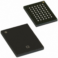
Package Diagrams Figure 8. 48-Pin VFBGA ( mm) (51-85150) Document #: 38-05569 Rev. *D ® CY62136EV30 MoBL 51-85150-*F Page [+] Feedback ...
Page 13
Package Diagrams (continued) Acronyms Acronym Description CMOS complementary metal oxide semiconductor I/O input/output SRAM static random access memory VFBGA very fine ball gird array TSOP thin small outline package Document #: 38-05569 Rev. *D Figure 9. 44-Pin TSOP II (51-85087) ...
Page 14
... Static RAM Date Description of Change New Data Sheet Converted from Advanced Information to Final. Changed the address of Cypress Semiconductor Corporation on Page #1 from “3901 North First Street” to “198 Champion Court” Removed 35ns Speed Bin Removed “L” version of CY62136EV30 Changed I (Max) value from ...
Page 15
... Cypress against all charges. Any Source Code (software and/or firmware) is owned by Cypress Semiconductor Corporation (Cypress) and is protected by and subject to worldwide patent protection (United States and foreign), United States copyright laws and international treaty provisions. Cypress hereby grants to licensee a personal, non-exclusive, non-transferable license to copy, use, modify, create derivative works of, and compile the Cypress Source Code and derivative works for the sole purpose of creating custom software and or firmware in support of licensee product to be used only in conjunction with a Cypress integrated circuit as specified in the applicable agreement ...