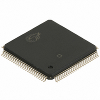
CY7C09099V-12AXC Cypress Semiconductor Corp, CY7C09099V-12AXC Datasheet - Page 2

CY7C09099V-12AXC
Manufacturer Part Number
CY7C09099V-12AXC
Description
CY7C09099V-12AXC
Manufacturer
Cypress Semiconductor Corp
Datasheet
1.CY7C09089V-12AXC.pdf
(21 pages)
Specifications of CY7C09099V-12AXC
Format - Memory
RAM
Memory Type
SRAM - Dual Port, Synchronous
Memory Size
1M (128K x 8)
Speed
12ns
Interface
Parallel
Voltage - Supply
3 V ~ 3.6 V
Operating Temperature
0°C ~ 70°C
Package / Case
100-LQFP
Lead Free Status / RoHS Status
Lead free / RoHS Compliant
Available stocks
Company
Part Number
Manufacturer
Quantity
Price
Company:
Part Number:
CY7C09099V-12AXC
Manufacturer:
Cypress Semiconductor Corp
Quantity:
10 000
Functional Description
The CY7C09079V/89V/99V and CY7C09179V/89V/99V are
high speed synchronous CMOS 32K, 64K, and 128K x 8/9
dual-port static RAMs. Two ports are provided, permitting
independent, simultaneous access for reads and writes to any
location in memory.
lines enable minimal setup and hold times. In pipelined output
mode, data is registered for decreased cycle time. Clock to data
valid t
used to bypass the pipelined output register to eliminate access
latency. In flow-through mode, data is available t
the address is clocked into the device. Pipelined output or
flow-through mode is selected via the FT/Pipe pin.
Each port contains a burst counter on the input address register.
The internal write pulse width is independent of the
LOW-to-HIGH transition of the clock signal. The internal write
pulse is self-timed to enable the shortest possible cycle times.
Pin Configurations
Notes
Document #: 38-06043 Rev. *C
4. When writing simultaneously to the same location, the final value cannot be guaranteed.
5. This pin is NC for CY7C09079V.
6. This pin is NC for CY7C09079V and CY7C09089V.
7. For CY7C09079V and CY7C09089V, pin #23 connected to V
compatible with an IDT 5V x16 flow-through device.
CD2
Figure 1. 100-Pin TQFP (Top View) - CY7C09099V (128K x 8), CY7C09089V (64K x 8),CY7C09079V (32K x 8)
= 6.5 ns
[7]
CNTRSTL
FT/PIPEL
[1]
[6]
[5]
CE0L
CE1L
R/WL
[4]
A10L
A11L
A12L
A13L
A14L
A15L
A16L
(pipelined). Flow-through mode can also be
VCC
OEL
A7L
A8L
A9L
NC
NC
NC
NC
NC
NC
NC
NC
Registers on control, address, and data
1
2
3
4
5
6
7
8
9
10
11
12
13
14
15
16
17
18
19
20
21
22
23
24
25
100
26
99
27
98
28
97
29
96
30
95
31
CD1
94
32
CC
= 18 ns after
93
33
is pin compatible with an IDT 5V x8 pipelined device; connecting pin #23 and #53 to GND is pin
92 91 90
34 35 36
89
37
88
38
A HIGH on CE
the internal circuitry to reduce the static power consumption. The
use of multiple Chip Enables enables easier banking of multiple
chips for depth expansion configurations. In the pipelined mode,
one cycle is required with CE
the outputs.
Counter enable inputs are provided to stall the operation of the
address input and use the internal address generated by the
internal counter for fast interleaved memory applications. A
port’s burst counter is loaded with the port’s Address Strobe
(ADS). When the port’s Count Enable (CNTEN) is asserted, the
address counter increments on each LOW-to-HIGH transition of
that port’s clock signal. This reads/writes one word from/into
each successive address location until CNTEN is deasserted.
The counter can address the entire memory array and loops
back to the start. Counter Reset (CNTRST) is used to reset the
burst counter.
All parts are available in 100-pin Thin Quad Plastic Flatpack
(TQFP) packages.
87 86
39 40
85
41
84
42
83 82 81
43 44 45
0
or LOW on CE
80
46
79
47
78 77
48 49
CY7C09079V/89V/99V
CY7C09179V/89V/99V
0
1
LOW and CE
76
50
for one clock cycle powers down
75
74
73
72
71
70
69
68
67
66
65
64
63
62
61
60
59
58
57
56
55
54
53
52
51
NC
NC
A7R
A8R
A9R
A10R
A11R
A12R
A13R
A14R
A15R
A16R
GND
NC
NC
NC
NC
CE0R
CE1R
CNTRSTR
R/WR
OER
FT/PIPER
GND
NC
1
HIGH to reactivate
[6]
[5]
[7]
Page 2 of 21
[+] Feedback


