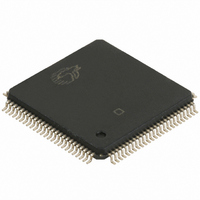
CY7C09099V-12AXC Cypress Semiconductor Corp, CY7C09099V-12AXC Datasheet - Page 4

CY7C09099V-12AXC
Manufacturer Part Number
CY7C09099V-12AXC
Description
CY7C09099V-12AXC
Manufacturer
Cypress Semiconductor Corp
Datasheet
1.CY7C09089V-12AXC.pdf
(21 pages)
Specifications of CY7C09099V-12AXC
Format - Memory
RAM
Memory Type
SRAM - Dual Port, Synchronous
Memory Size
1M (128K x 8)
Speed
12ns
Interface
Parallel
Voltage - Supply
3 V ~ 3.6 V
Operating Temperature
0°C ~ 70°C
Package / Case
100-LQFP
Lead Free Status / RoHS Status
Lead free / RoHS Compliant
Available stocks
Company
Part Number
Manufacturer
Quantity
Price
Company:
Part Number:
CY7C09099V-12AXC
Manufacturer:
Cypress Semiconductor Corp
Quantity:
10 000
Selection Guide
Pin Definitions
Document #: 38-06043 Rev. *C
f
(Pipelined)
Max. Access Time
(ns) (Clock to Data,
Pipelined)
Typical Operating
Current I
Typical Standby
Current for I
(mA) (Both Ports
TTL Level)
Typical Standby
Current for I
(μA) (Both Ports
CMOS Level)
A
ADS
CE
CLK
CNTEN
CNTRST
I/O
OE
R/W
FT/PIPE
GND
NC
V
Notes
MAX2
8. This pin is NC for CY7C09179V.
9. This pin is NC for CY7C09179V and CY7C09189V
0L
CC
0L
0L
L
Description
–A
L
L
L
–I/O
,CE
Left Port
(MHz)
16L
L
L
CC
1L
L
8L
(mA)
SB1
SB3
CY7C09179V/89V/99V-6
A
ADS
CE
CLK
CNTEN
CNTRST
I/O
OE
R/W
FT/PIPE
Right Port
0R
CY7C09079V/89V/99V
0R
0R
R
–A
R
R
R
–I/O
,CE
16R
R
1R
R
R
8R
10 μA
100
175
6.5
25
Address Inputs (A
Address Strobe Input. Used as an address qualifier. This signal should be asserted LOW to
access the part using an externally supplied address. Asserting this signal LOW also loads
the burst counter with the address present on the address pins.
Chip Enable Input. To select either the left or right port, both CE
to their active states (CE
Clock Signal. This input can be free running or strobed. Maximum clock input rate is f
Counter Enable Input. Asserting this signal LOW increments the burst address counter of its
respective port on each rising edge of CLK. CNTEN is disabled if ADS or CNTRST are
asserted LOW.
Counter Reset Input. Asserting this signal LOW resets the burst address counter of its
respective port to zero. CNTRST is not disabled by asserting ADS or CNTEN.
Data Bus Input/Output (I/O
Output Enable Input. This signal must be asserted LOW to enable the I/O data pins during
read operations.
Read/Write Enable Input. This signal is asserted LOW to write to the dual port memory array.
For read operations, assert this pin HIGH.
Flow-Through/Pipelined Select Input. For flow-through mode operation, assert this pin LOW.
For pipelined mode operation, assert this pin HIGH.
Ground Input.
No Connect.
Power Input.
[1]
CY7C09179V/89V/99V-7
CY7C09079V/89V/99V
0
–A
14
for 32K; A
0
10 μA
155
7.5
≤ V
83
25
0
–I/O
IL
and CE
7
for x8 devices; I/O
0
–A
15
[1]
1
Description
for 64K; and A
≥ V
CY7C09079V/89V/99V
CY7C09179V/89V/99V
IH
).
0
10 μA
–I/O
135
67
20
-9
9
0
–A
8
CY7C09079V/89V/99V
CY7C09179V/89V/99V
for x9 devices).
16
for 128K devices).
0
AND CE
CY7C09079V/89V/99V
CY7C09179V/89V/99V
1
must be asserted
10 μA
115
-12
50
12
20
Page 4 of 21
MAX
.
[+] Feedback


