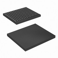
CY7C1315BV18-250BZXC Cypress Semiconductor Corp, CY7C1315BV18-250BZXC Datasheet - Page 12

CY7C1315BV18-250BZXC
Manufacturer Part Number
CY7C1315BV18-250BZXC
Description
SRAM (Static RAM)
Manufacturer
Cypress Semiconductor Corp
Datasheet
1.CY7C1315BV18-200BZXC.pdf
(32 pages)
Specifications of CY7C1315BV18-250BZXC
Format - Memory
RAM
Memory Type
SRAM - Synchronous, QDR II
Memory Size
18M (512K x 36)
Speed
250MHz
Interface
Parallel
Voltage - Supply
1.7 V ~ 1.9 V
Operating Temperature
0°C ~ 70°C
Package / Case
165-LFBGA
Lead Free Status / RoHS Status
Lead free / RoHS Compliant
Available stocks
Company
Part Number
Manufacturer
Quantity
Price
Company:
Part Number:
CY7C1315BV18-250BZXC
Manufacturer:
Cypress Semiconductor Corp
Quantity:
135
Company:
Part Number:
CY7C1315BV18-250BZXC
Manufacturer:
Cypress Semiconductor Corp
Quantity:
10 000
Write Cycle Descriptions
The write cycle description table for CY7C1311BV18 and CY7C1313BV18 follows.
Write Cycle Descriptions
The write cycle description table for CY7C1911BV18 follows.
Note
Document Number: 38-05620 Rev. *F
10. Is based on a write cycle that was initiated in accordance with the
BWS
NWS
BWS
H
H
H
H
different portions of a write cycle, as long as the setup and hold requirements are achieved.
H
H
L
L
L
L
L
L
0
0
0
/
BWS
NWS
L–H
L–H
H
H
H
H
L
L
L
L
K
–
–
1
1
/
L–H
L–H
L–H
L–H
K
–
–
–
–
L–H
L–H
K
–
–
L–H During the data portion of a write sequence
L–H During the data portion of a write sequence
L–H No data is written into the devices during this portion of a write operation.
L-H During the data portion of a write sequence
K
–
–
–
–
During the data portion of a write sequence, the single byte (D
During the data portion of a write sequence, the single byte (D
No data is written into the device during this portion of a write operation.
No data is written into the device during this portion of a write operation.
During the data portion of a write sequence
CY7C1311BV18 both nibbles (D
CY7C1313BV18 both bytes (D
CY7C1311BV18 both nibbles (D
CY7C1313BV18 both bytes (D
During the data portion of a write sequence
CY7C1311BV18 only the lower nibble (D
CY7C1313BV18 only the lower byte (D
CY7C1311BV18 only the lower nibble (D
CY7C1313BV18 only the lower byte (D
During the data portion of a write sequence
CY7C1311BV18 only the upper nibble (D
CY7C1313BV18 only the upper byte (D
CY7C1311BV18 only the upper nibble (D
CY7C1313BV18 only the upper byte (D
No data is written into the devices during this portion of a write operation.
Write Cycle Descriptions
[2, 10]
[17:0]
[17:0]
[7:0]
[7:0]
) are written into the device.
) are written into the device.
) are written into the device.
) are written into the device.
[8:0]
[8:0]
[17:9]
[17:9]
[3:0]
[3:0]
Comments
[7:4]
[7:4]
table. NWS
Comments
) is written into the device, D
) is written into the device, D
CY7C1313BV18, CY7C1315BV18
CY7C1311BV18, CY7C1911BV18
) is written into the device, D
) is written into the device, D
) is written into the device, D
) is written into the device, D
) is written into the device, D
) is written into the device, D
[2, 10]
0
, NWS
1
[8:0]
[8:0]
, BWS
) is written into the device.
) is written into the device.
0
, BWS
1
, BWS
[17:9]
[17:9]
[8:0]
[8:0]
[7:4]
[7:4]
[3:0]
[3:0]
2
, and BWS
remains unaltered.
remains unaltered.
remains unaltered.
remains unaltered.
remains unaltered.
remains unaltered.
remains unaltered.
remains unaltered.
3
can be altered on
Page 12 of 32
[+] Feedback


