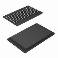
CY7C1361C-100BGC Cypress Semiconductor Corp, CY7C1361C-100BGC Datasheet - Page 9

CY7C1361C-100BGC
Manufacturer Part Number
CY7C1361C-100BGC
Description
SRAM (Static RAM)
Manufacturer
Cypress Semiconductor Corp
Datasheet
1.CY7C1361C-133AJXC.pdf
(34 pages)
Specifications of CY7C1361C-100BGC
Format - Memory
RAM
Memory Type
SRAM - Synchronous
Memory Size
9M (256K x 36)
Speed
100MHz
Interface
Parallel
Voltage - Supply
3.135 V ~ 3.6 V
Operating Temperature
0°C ~ 70°C
Package / Case
119-BGA
Lead Free Status / RoHS Status
Contains lead / RoHS non-compliant
Available stocks
Company
Part Number
Manufacturer
Quantity
Price
Company:
Part Number:
CY7C1361C-100BGC
Manufacturer:
Cypress Semiconductor Corp
Quantity:
10 000
Company:
Part Number:
CY7C1361C-100BGCT
Manufacturer:
Cypress Semiconductor Corp
Quantity:
10 000
Pin Definitions
Document Number: 38-05541 Rev. *J
MODE
V
V
V
V
TDO
TDI
TMS
TCK
NC
V
DD
DDQ
SS
SSQ
SS
/DNU
Name
JTAG serial output
I/O power supply Power supply for the I/O circuitry.
JTAG serial input
JTAG serial input
(continued)
Power supply
Ground/DNU
synchronous
synchronous
synchronous
I/O ground
Ground
JTAG-
Input-
static
clock
I/O
–
Selects burst order. When tied to GND selects linear burst sequence. When tied to V
or left floating selects interleaved burst sequence. This is a strap pin and should remain
static during device operation. Mode Pin has an internal pull-up.
Power supply inputs to the core of the device.
Ground for the core of the device.
Ground for the I/O circuitry.
Serial data-out to the JTAG circuit. Delivers data on the negative edge of TCK. If the
JTAG feature is not being used, this pin should be left unconnected. This pin is not
available on TQFP packages.
Serial data-in to the JTAG circuit. Sampled on the rising edge of TCK. If the JTAG
feature is not being used, this pin can be left floating or connected to V
up resistor. This pin is not available on TQFP packages.
Serial data-in to the JTAG circuit. Sampled on the rising edge of TCK. If the JTAG
feature is not being used, this pin can be disconnected or connected to V
not available on TQFP packages.
Clock input to the JTAG circuitry. If the JTAG feature is not being used, this pin must
be connected to V
No connects. Not internally connected to the die. 18M, 36M, 72M, 144M, 288M, 576M,
and 1G are address expansion pins and are not internally connected to the die.
This pin can be connected to ground or should be left floating.
SS
. This pin is not available on TQFP packages.
Description
CY7C1361C/CY7C1363C
DD
DD
through a pull
. This pin is
Page 9 of 34
DD
[+] Feedback


