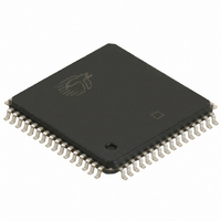
CY7C4225-15AXC Cypress Semiconductor Corp, CY7C4225-15AXC Datasheet - Page 3

CY7C4225-15AXC
Manufacturer Part Number
CY7C4225-15AXC
Description
CY7C4225-15AXC
Manufacturer
Cypress Semiconductor Corp
Series
CY7Cr
Datasheet
1.CY7C4225-15AXC.pdf
(22 pages)
Specifications of CY7C4225-15AXC
Function
Synchronous
Memory Size
18K (1K x 18)
Data Rate
100MHz
Access Time
10ns
Voltage - Supply
3.3V
Operating Temperature
-40°C ~ 85°C
Mounting Type
Surface Mount
Package / Case
64-LQFP
Lead Free Status / RoHS Status
Lead free / RoHS Compliant
Other names
428-1758
CY7C4225-15AXC
CY7C4225-15AXC
Available stocks
Company
Part Number
Manufacturer
Quantity
Price
Company:
Part Number:
CY7C4225-15AXC
Manufacturer:
Cypress Semiconductor Corp
Quantity:
10 000
Company:
Part Number:
CY7C4225-15AXCT
Manufacturer:
Cypress Semiconductor Corp
Quantity:
10 000
Selection Guide
Pin Definitions
Document Number: 001-45652 Rev. *A
Maximum Frequency (MHz)
Maximum Access Time (ns)
Minimum Cycle Time (ns)
Minimum Data or Enable Set-Up (ns)
Minimum Data or Enable Hold (ns)
Maximum Flag Delay (ns)
Operating Current (I
Density
Packages
D
Q
WEN
REN
WCLK
RCLK
WXO/HF
EF
FF
PAE
PAF
LD
FL/RT
WXI
RXI
Signal Name
0−17
0−17
Parameter
(14 x 14, 10 x 10)
Data Inputs
Data Outputs
Write Enable
Read Enable
Write Clock
Read Clock
Write Expansion
Out/Half Full Flag
Empty Flag
Full Flag
Programmable
Almost Empty
Programmable
Almost Full
Load
First Load/
Retransmit
Write Expansion
Input
Read Expansion
Input
64-pin TQFP
68-pin PLCC
CY7C4425
CC2
Description
(10 x 10)
64 x 18
Description
) (mA) @ 20MHz
(14 x 14, 10 x 10)
64-pin TQFP
68-pin PLCC
IO
O
O
O
O
O
O
CY7C4205
I
I
I
I
I
I
I
I
I
(10 x 10)
256 x 18
Data inputs for an 18-bit bus.
Data outputs for an 18-bit bus.
Enables the WCLK input.
Enables the RCLK input.
The rising edge clocks data into the FIFO when WEN is LOW and the FIFO is not Full.
When LD is asserted, WCLK writes data into the programmable flag-offset register.
The rising edge clocks data out of the FIFO when REN is LOW and the FIFO is not
Empty. When LD is asserted, RCLK reads data out of the programmable flag-offset
register.
Dual-Mode Pin. Single device or width expansion - Half Full status flag. Cascaded – Write
Expansion Out signal, connected to WXI of next device.
When EF is LOW, the FIFO is empty. EF is synchronized to RCLK.
When FF is LOW, the FIFO is full. FF is synchronized to WCLK.
When PAE is LOW, the FIFO is almost empty based on the almost empty offset value
programmed into the FIFO. PAE is asynchronous when V
it is synchronized to RCLK when V
When PAF is LOW, the FIFO is almost full based on the almost full offset value
programmed into the FIFO. PAF is asynchronous when V
it is synchronized to WCLK when V
When LD is LOW, D
mable-flag-offset register.
Dual-Mode Pin. Cascaded – The first device in the daisy chain will have FL tied to V
all other devices will have FL tied to V
is tied to V
available in standalone mode by strobing RT.
Cascaded – Connected to WXO of previous device. Not Cascaded – Tied to V
Cascaded – Connected to RXO of previous device. Not Cascaded – Tied to V
Commercial
Industrial
SS
(14 x 14, 10 x 10)
on all devices. Not Cascaded – Tied to V
64-pin TQFP
68-pin PLCC
CY7C4215
(10 x 10)
512 x 18
0−17
100
-10
0.5
10
45
50
8
3
8
(O
0−17
(14 x 14, 10 x 10)
) are written (read) into (from) the program-
64-pin TQFP
68-pin PLCC
CY7C4225
(10 x 10)
1K x 18
CC
CC
Function
/SMODE is tied to V
/SMODE is tied to V
CC
66.7
-15
15
50
10
10
45
4
1
. In standard mode of width expansion, FL
(14 x 14, 10 x 10)
CY7C4425/4205/4215
CY7C4225/4235/4245
64-pin TQFP
68-pin PLCC
CY7C4235
(10 x 10)
SS
2K x 18
. Retransmit function is also
-25
40
15
25
15
45
50
CC
CC
6
1
SS
SS
/SMODE is tied to V
/SMODE is tied to V
.
.
(14 x 14, 10 x 10)
64-pin TQFP
68-pin PLCC
CY7C4245
(10 x 10)
4K x 18
Page 3 of 22
28.6
-35
35
50
20
20
45
7
2
SS
SS
.
.
CC
CC
SS
;
;
;
[+] Feedback


