MT9M001C12STM Aptina LLC, MT9M001C12STM Datasheet
MT9M001C12STM
Specifications of MT9M001C12STM
Q3930625
Q3990821
Available stocks


Related parts for MT9M001C12STM


MT9M001C12STM Summary of contents
Page 1
... Megapixel CMOS Digital Image Sensor MT9M001C12STM (Monochrome) For the latest data sheet, refer to Micron’s Web site: Features ® • Micron DigitalClarity™ CMOS imaging technology • Array Format (5:4): 1,280H x 1,024V (1,310,720 active pixels). Total (incl. dark pixels): 1,312H x 1,048V (1,374,976 pixels) • ...
Page 2
Table of Contents Applications . . . . . . . . . . . . . . . . . . . . . . . . . . . . . . . . . . . . ...
Page 3
List of Tables Table 1: Key Performance Parameters ...
Page 4
List of Figures Figure 1: 48-Pin CLCC Package Pinout Diagram . . . . . . . . . . . . . . . . . . . . . . . . . . . . . . ...
Page 5
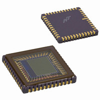
General Description Figure 1: 48-Pin CLCC Package Pinout Diagram STANDBY TRIGGER RESET# OE# A GND V A GND A GND Figure 2: Block Diagram 1,280H x 1,024V Analog Processing PDF: 09005aef81c2856f/Source: 09005aef80a3e031 MT9M001_DS_2.fm - Rev. F 5/06 EN MT9M001: 1/2-Inch ...
Page 6
Table 3: Pin Descriptions Pin Numbers Symbol 29 CLKIN 13 OE# 10 RESET# 46 SCLK 7 STANDBY 8 TRIGGER 45 S DATA 24–28, 32–36 D <0–9> OUT 41 FRAME_VALID 40 LINE_VALID 31 PIXCLK 39 STROBE 15,17,18,21, 47, A GND 48 ...
Page 7
Pixel Data Format Pixel Array Structure The MT9M001 pixel array is configured as 1,312 columns by 1,048 rows (shown in Figure 3). The first 16 columns and the first eight rows of pixels are optically black, and can be used ...
Page 8
Output Data Format The MT9M001 image data is read out in a progressive scan. Valid image data is surrounded by horizontal blanking and vertical blanking, as shown in Figure 5. The amount of horizontal blanking and vertical blanking is programmable ...
Page 9
Figure 7: Row Timing and FRAME_VALID/LINE_VALID Signals FRAME_VALID LINE_VALID Number of master clocks PDF: 09005aef81c2856f/Source: 09005aef80a3e031 MT9M001_DS_2.fm - Rev. F 5/06 EN MT9M001: 1/2-Inch Megapixel Digital Image Sensor . . . . . . . . . ...
Page 10
Frame Timing Formulas Table 4: Frame Timing Parameter Name A Active Data Time P Frame Start Blanking (242 Frame End Blanking Horizontal Blanking Row Time V Vertical ...
Page 11
Serial Bus Description Registers are written to and read from the MT9M001 through the two-wire serial inter- face bus. The sensor is a two-wire serial interface slave and is controlled by the serial clock (SCLK), which is driven by the ...
Page 12
Stop Bit The stop bit is defined as a LOW-to-HIGH transition of the data line while the clock line is HIGH. Slave Address The 8-bit address of a two-wire serial interface device consists of seven bits of address and 1 ...
Page 13
Two-Wire Serial Interface Sample Write and Read Sequences 16-Bit Write Sequence A typical write sequence for writing 16 bits to a register is shown in Figure 8. A start bit given by the master, followed by the write address, starts ...
Page 14
Registers Register Map Table 6: Register List and Default Values Register # (Hex) Description 0x00 Chip Version 0x01 Row Start 0x02 Column Start 0x03 Row Size (Window Height) 0x04 Col Size (Window Width) 0x05 Horizontal Blanking 0x06 Vertical Blanking 0x07 ...
Page 15
Table 7: Register Description Register Bit Chip ID 0x00 15:0 This register is read-only and gives the chip identification number: 0x8431. Window Control These registers control the size of the window. 0x01 10:0 First row to be read out 0x02 ...
Page 16
Table 7: Register Description (continued) Register Bit Pixel Integration Control These registers (along with the window sizing and blanking registers) control the integration time for the pixels. The actual total integration time ( t INT = Reg0x09 x row time ...
Page 17
Table 7: Register Description (continued) Register Bit Read Mode 1 In read mode 1, this register is used to control many aspects of the readout of the sensor. — 0x1E 0 Reserved 1 — Reserved 2 Column Skip 4 1 ...
Page 18
Table 7: Register Description (continued) Register Bit 0x2D 6:0 Even row, odd column 0x2E 6:0 Odd row, odd column 0x35 6:0 Global gain Test Data 0x32 11:2 Test Data. The value used to produce a test pattern in “Use Test ...
Page 19
Table 7: Register Description (continued) Register Bit — 0x5F 5:0 Thres_lo Lower threshold for black level in ADC LSBs override automatic Thres_hi and Thres_lo adjust (Thres_hi always = bits 14:8; Thres_lo always = bits 5:0). Default = ...
Page 20
Table 7: Register Description (continued) Register Bit Chip Enable and Two-Wire Serial Interface Write Synchronize. 0xF1 0 Mirrors the functionality of Reg0x07 bit1 (Chip Enable normal operation stop sensor readout; when this is returned to “1,” ...
Page 21
Feature Description Signal Path The MT9M001 signal path consists of two stages, a programmable gain stage and a programmable analog offset stage. Programmable Gain Stage A total programmable gain available and can be calculated using the following ...
Page 22
Programmable Analog Offset Stage The programmable analog offset stage corrects for analog offset that might be present in the analog signal. The user would need to program register 0x62 appropriately to enable the analog offset correction. The lower eight bits ...
Page 23
Figure 13: Readout of Eight Pixels in Normal and Column Skip Output Mode Normal readout Column skip readout Black Level Calibration The MT9M001 has automatic black level calibration on-chip which can be overridden by the user, as described below and ...
Page 24
Figure 14: Black Level Calibration Flow Chart Pixel Output (signal minus PDF: 09005aef81c2856f/Source: 09005aef80a3e031 MT9M001_DS_2.fm - Rev. F 5/06 EN MT9M001: 1/2-Inch Megapixel Digital Image Sensor Gain Selection (color-wise 10-bit ADC reset) Offset Correction Voltage (color-wise) Micron Technology, ...
Page 25
Registers Table 9: Black Level Registers Register bit Description Reg0x5F This register controls the operation of the black level calibration thresholds gain dependence Thres_lo is set by the programmed value of bits 5:0, Thres_hi is reset ...
Page 26
Registers Table 9: Black Level Registers (continued) Register bit Description Reg0x60, These registers contain the 9-bit signed black level calibration values. In normal operation, these Reg0x61, values are calculated at the beginning of each frame. However, if Reg0x62, bit 0 ...
Page 27
Still Image Capture with External Synchronization In continuous mode video image capture, the TRIGGER signal should be held LOW or “0.” To capture a still image, the sensor must first be put into snapshot mode by programming a “1” in ...
Page 28
Electrical Specifications Data Output and Propagation Delays By default, the MT9M001 launches pixel data, FRAME_VALID and LINE_VALID with the rising edge of PIXCLK. The expectation is that the user captures D FRAME_VALID and LINE_VALID using the falling edge of PIXCLK. ...
Page 29
Table 10: DC Electrical Characteristics (continued) (DC Setup Conditions: Symbol Definition I Pixel supply current AAPIX I Digital standby current STDBYD I Digital standby current STDBYD /CLK W I Analog standby current STDBYDA . Table 11: AC Electrical Characteristics (AC ...
Page 30
Two-wire Serial Bus Timing The two-wire serial bus operation requires certain minimum master clock cycles between transitions. These are specified in the following diagrams in master clock cycles. Figure 18: Serial Host Interface Start Condition Timing SCLK S DATA Figure ...
Page 31
Figure 22: Acknowledge Signal Timing After an 8-Bit Write to the Sensor SCLK S DATA Figure 23: Acknowledge Signal Timing After an 8-Bit Read from the Sensor SCLK S DATA Note: After a read, the master receiver must pull down ...
Page 32
Quantum Efficiency Figure 24: Quantum Efficiency—Monochrome Image Center Offset and Orientation Figure 25: Image Center Offset 7.75mm Die Center PDF: 09005aef81c2856f/Source: 09005aef80a3e031 MT9M001_DS_2.fm - Rev. F 5/06 EN MT9M001: 1/2-Inch Megapixel Digital Image ...
Page 33
Table 13: Optical Area Dimensions Optical Area SXGA Center of pixel (20, 12) Center of Pixel (1299, 1035) Chip Size, mm (including Seal Ring) Notes and Y coordinates referenced to center of die. 2. Die center = package ...
Page 34
Figure 27: 48-pin CLCC Package Outline Drawing D SEATING PLANE A 11.176 1.016 TYP 48 1 48X 0.50 11.176 5.588 5.588 7.11 14.220 +0.300 -0.125 NOTE: 1. THESE DIMENSIONS ARE NON ACCUMULATIVE Note: All dimensions in millimeters. 8000 S. Federal ...
Page 35
Revision History Rev ...