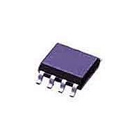
TISP7180F3D-S Bourns Inc., TISP7180F3D-S Datasheet - Page 18

TISP7180F3D-S
Manufacturer Part Number
TISP7180F3D-S
Description
Sidacs Triple Element Bidirectional
Manufacturer
Bourns Inc.
Datasheet
1.TISP7125F3DR.pdf
(19 pages)
Specifications of TISP7180F3D-S
Breakover Current Ibo Max
4.3 A
Rated Repetitive Off-state Voltage Vdrm
145 V
Off-state Leakage Current @ Vdrm Idrm
0.01 mA
Forward Voltage Drop
5 V
Mounting Style
SMD/SMT
Package / Case
SO-8
Lead Free Status / RoHS Status
Lead free / RoHS Compliant
Available stocks
Company
Part Number
Manufacturer
Quantity
Price
Part Number:
TISP7180F3D-S
Manufacturer:
TI/德州仪器
Quantity:
20 000
The protection voltage, (V (BO) ), increases under lightning surge conditions due to thyristor regeneration. This increase is dependent on the
rate of current rise, di/dt, when the TISP ® device is clamping the voltage in its breakdown region. The V (BO) value under surge conditions can
be estimated by multiplying the 50 Hz rate V (BO) (250 V/ms) value by the normalized increase at the surge’s di/dt. An estimate of the di/dt can
be made from the surge generator voltage rate of rise, dv/dt, and the circuit resistance.
As an example, the ITU-T recommendation K.21 1.5 kV, 10/700 surge has an average dv/dt of 150 V/µs, but, as the rise is exponential, the
initial dv/dt is three times higher, being 450 V/µs. The instantaneous generator output resistance is 25 Ω. If the equipment has an additional
series resistance of 20 Ω, the total series resistance becomes 45 Ω. The maximum di/dt then can be estimated as 450/45 = 10 A/µs. In
practice, the measured di/dt and protection voltage increase will be lower due to inductive effects and the finite slope resistance of the TISP ®
breakdown region.
The off-state capacitance of a TISP ® device is sensitive to junction temperature, T J , and the bias voltage, comprising of the dc voltage, V D ,
and the ac voltage, V d . All the capacitance values in this data sheet are measured with an ac voltage of 1 Vrms. When V D >> V d , the capaci-
tance value is independent on the value of V d . Up to 10 MHz, the capacitance is essentially independent of frequency. Above 10 MHz, the
effective capacitance is strongly dependent on connection inductance. For example, a printed wiring (PW) trace of 10 cm could create a circuit
resonance with the device capacitance in the region of 80 MHz.
Longitudinal Balance
Figure 35 shows a three terminal TISP ® device with its equivalent “delta” capacitance. Each capacitance, C TG , C RG and C TR , is the true
terminal pair capacitance measured with a three terminal or guarded capacitance bridge. If wire R is biased at a larger potential than wire T,
then C TG > C RG . Capacitance C TG is equivalent to a capacitance of C RG in parallel with the capacitive difference of (C TG -C RG ). The line
capacitive unbalance is due to (CTG -C RG ) and the capacitance shunting the line is C TR +C RG /2 .
All capacitance measurements in this data sheet are three terminal guarded to allow the designer to accurately assess capacitive unbalance
effects. Simple two terminal capacitance meters (unguarded third terminal) give false readings as the shunt capacitance via the third terminal is
included.
Off-State Capacitance
MARCH 1994 - REVISED SEPTEMBER 2008
Specifications are subject to change without notice.
Customers should verify actual device performance in their specific applications.
Protection Voltage
Capacitance
TISP7xxxF3 (MV, HV) Overvoltage Protector Series
APPLICATIONS INFORMATION
Figure 35.


