2N6507T ON Semiconductor, 2N6507T Datasheet - Page 2
2N6507T
Manufacturer Part Number
2N6507T
Description
SCRs 400V 25A
Manufacturer
ON Semiconductor
Datasheet
1.2N6505T.pdf
(7 pages)
Specifications of 2N6507T
Breakover Current Ibo Max
250 A
Rated Repetitive Off-state Voltage Vdrm
400 V
Off-state Leakage Current @ Vdrm Idrm
0.01 mA
Forward Voltage Drop
1.8 V
Gate Trigger Voltage (vgt)
1.5 V
Gate Trigger Current (igt)
30 mA
Holding Current (ih Max)
40 mA
Mounting Style
Through Hole
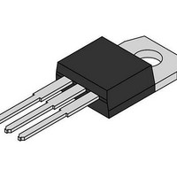
Package / Case
TO-220-3
Lead Free Status / RoHS Status
Lead free / RoHS Compliant
Available stocks
Company
Part Number
Manufacturer
Quantity
Price

Part Number:
2N6507TG
Manufacturer:
ON/安森美
Quantity:
20 000


Stresses exceeding Maximum Ratings may damage the device. Maximum Ratings are stress ratings only. Functional operation above the
Recommended Operating Conditions is not implied. Extended exposure to stresses above the Recommended Operating Conditions may affect
device reliability.
1. V
*Indicates JEDEC Registered Data.
2. Pulse Test: Pulse Width
MAXIMUM RATINGS
THERMAL CHARACTERISTICS
ELECTRICAL CHARACTERISTICS
OFF CHARACTERISTICS
ON CHARACTERISTICS
DYNAMIC CHARACTERISTICS
*Peak Repetitive Off-State Voltage (Note 1)
On‐State Current RMS (180 Conduction Angles; T
Average On‐State Current (180 Conduction Angles; T
Peak Non‐repetitive Surge Current (1/2 Cycle, Sine Wave 60 Hz, T
Forward Peak Gate Power (Pulse Width
Forward Average Gate Power (t = 8.3 ms, T
Forward Peak Gate Current (Pulse Width
Operating Junction Temperature Range
Storage Temperature Range
*Thermal Resistance, Junction-to-Case
*Maximum Lead Temperature for Soldering Purposes 1/8 in from Case for 10 Seconds
* Peak Repetitive Forward or Reverse Blocking Current
* Forward On-State Voltage (Note 2) (I
* Gate Trigger Current (Continuous dc)
* Gate Trigger Voltage (Continuous dc) (V
* Holding Current
* Turn‐On Time (I
Critical Rate of Rise of Off‐State Voltage (Gate Open, Rated V
Gate Non‐Trigger Voltage (V
Turn‐Off Time (V
voltage shall not be applied concurrent with negative potential on the anode. Blocking voltages shall not be tested with a constant current
source such that the voltage ratings of the devices are exceeded.
(Gate Open, Sine Wave 50 to 60 Hz, T
(V
(V
(V
(I
(I
DRM
TM
TM
AK
AK
AK
= 25 A, I
= 25 A, I
and V
= Rated V
= 12 Vdc, R
= 12 Vdc, Initiating Current = 200 mA, Gate Open) T
RRM
R
R
DRM
TM
= 25 A)
= 25 A, T
DRM
for all types can be applied on a continuous basis. Ratings apply for zero or negative gate voltage; however, positive gate
L
= 25 A, I
= 100 W)
= rated voltage)
or V
(T
J
RRM
J
= 25 C unless otherwise noted)
300 ms, Duty Cycle
= 125 C)
AK
GT
, Gate Open)
= 12 Vdc, R
= 50 mAdc)
Characteristic
Characteristic
2N6504
2N6505
2N6507
2N6508
2N6509
TM
Rating
(T
J
AK
= 50 A)
C
1.0 ms, T
= 25 to 125 C)
1.0 ms, T
C
= 25 C unless otherwise noted.)
L
= 12 Vdc, R
= 85 C)
= 100 W, T
2%.
C
C
C
= 85 C)
C
= 85 C)
= 85 C)
= 85 C)
J
L
http://onsemi.com
2N6504 Series
= 125 C)
T
T
T
T
= 100 W, T
T
DRM
J
J
C
C
C
C
= 25 C
= 125 C
= 25 C
= -40 C
= 25 C
= -40 C
, Exponential Waveform)
J
2
= 100 C)
C
= -40 C)
Symbol
Symbol
I
R
I
dv/dt
Symbol
DRM
V
V
V
I
RRM
I
V
P
T
V
T(RMS)
t
I
GT
I
qJC
t
I
TM
GT
GD
P
H
gt
T(AV)
q
I
T
DRM,
TSM
G(AV)
L
RRM
GM
T
GM
stg
J
,
Min
0.2
-
-
-
-
-
-
-
-
-
-
-
-
-40 to +125
-40 to +150
Value
Max
100
400
600
800
250
260
Typ
0.5
2.0
1.5
9.0
1.0
1.5
50
25
16
20
18
15
35
50
-
-
-
-
-
-
Max
2.0
1.8
1.5
2.0
10
30
75
40
80
-
-
-
-
Unit
W
W
V
A
A
A
A
V/ms
C
C
Unit
Unit
C/W
mA
mA
mA
mA
ms
ms
V
V
V
C
Related parts for 2N6507T
Image
Part Number
Description
Manufacturer
Datasheet
Request
R

Part Number:
Description:
ON Semiconductor [VOLTAGE REGULATOR]
Manufacturer:
ON Semiconductor
Datasheet:
Part Number:
Description:
357-036-542-201 CARDEDGE 36POS DL .156 BLK LOPRO
Manufacturer:
ON Semiconductor
Datasheet:
Part Number:
Description:
357-036-542-201 CARDEDGE 36POS DL .156 BLK LOPRO
Manufacturer:
ON Semiconductor
Datasheet:
Part Number:
Description:
357-036-542-201 CARDEDGE 36POS DL .156 BLK LOPRO
Manufacturer:
ON Semiconductor
Datasheet:
Part Number:
Description:
357-036-542-201 CARDEDGE 36POS DL .156 BLK LOPRO
Manufacturer:
ON Semiconductor
Datasheet:
Part Number:
Description:
357-036-542-201 CARDEDGE 36POS DL .156 BLK LOPRO
Manufacturer:
ON Semiconductor
Datasheet:
Part Number:
Description:
357-036-542-201 CARDEDGE 36POS DL .156 BLK LOPRO
Manufacturer:
ON Semiconductor
Datasheet:
Part Number:
Description:
357-036-542-201 CARDEDGE 36POS DL .156 BLK LOPRO
Manufacturer:
ON Semiconductor
Datasheet:
Part Number:
Description:
357-036-542-201 CARDEDGE 36POS DL .156 BLK LOPRO
Manufacturer:
ON Semiconductor
Datasheet:
Part Number:
Description:
357-036-542-201 CARDEDGE 36POS DL .156 BLK LOPRO
Manufacturer:
ON Semiconductor
Datasheet:
Part Number:
Description:
357-036-542-201 CARDEDGE 36POS DL .156 BLK LOPRO
Manufacturer:
ON Semiconductor
Datasheet:
Part Number:
Description:
Manufacturer:
ON Semiconductor
Datasheet:
Part Number:
Description:
Manufacturer:
ON Semiconductor
Datasheet:
Part Number:
Description:
Manufacturer:
ON Semiconductor
Datasheet: