AOP610 Alpha & Omega Semiconductor Inc, AOP610 Datasheet
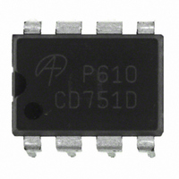
MOSFET N/P-CH COMPL 30V 8-PDIP

AOP610

Manufacturer Part Number
AOP610
Description
MOSFET N/P-CH COMPL 30V 8-PDIP
Manufacturer
Alpha & Omega Semiconductor Inc
Datasheet

Specifications of AOP610

Fet Type
N and P-Channel
Fet Feature
Logic Level Gate
Rds On (max) @ Id, Vgs
24 mOhm @ 7.7A, 10V
Drain To Source Voltage (vdss)
30V
Current - Continuous Drain (id) @ 25° C
7.7A, 6.2A
Vgs(th) (max) @ Id
3V @ 250µA
Gate Charge (qg) @ Vgs
15nC @ 10V
Input Capacitance (ciss) @ Vds
630pF @ 15V
Power - Max
2.3W
Mounting Type
Through Hole
Package / Case
8-DIP
Lead Free Status / RoHS Status
Lead free / RoHS Compliant
Other names
785-1143-1
785-1143-1
785-1143-5

Available stocks

Company
Part Number
Manufacturer
Quantity
Price
Part Number:
AOP610
Manufacturer:
ALPHA
Quantity:
20 000
Alpha & Omega Semiconductor, Ltd.
Absolute Maximum Ratings T
Parameter
Drain-Source Voltage
Gate-Source Voltage
Continuous Drain
Current
Pulsed Drain Current
Power Dissipation
Avalanche Current
Repetitive avalanche energy 0.3mH
Junction and Storage Temperature Range
Thermal Characteristics: n-channel+schottky and p-channel
Parameter
Maximum Junction-to-Ambient
Maximum Junction-to-Lead
Maximum Junction-to-Ambient
Maximum Junction-to-Lead
AOP610
Complementary Enhancement Mode Field Effect Transistor
General Description
The AOP610 uses advanced trench
technology MOSFETs to provide excellent
R
complementary MOSFETs may be used to
form a level shifted high side switch, and for a
host of other applications. A Schottky diode in
parallel with the n-channel FET reduces body
diode related losses. It is ESD protected.
Standard product AOP610 is Pb-free (meets
ROHS & Sony 259 specifications). AOP610L
is a Green Product ordering option. AOP610
and AOP610L are electrically identical.
DS(ON)
A
and low gate charge. The
S2/A
S1
G2
G1
PDIP-8
1
2
3
4
B
8
7
6
5
B
T
T
T
T
A
A
A
A
=25°C
=70°C
=25°C
=70°C
D2/K
D2/K
D1
D1
C
C
N-ch
P-ch
A
A
A
A
A
=25°C unless otherwise noted
B
Steady-State
Steady-State
Steady-State
Steady-State
t ≤ 10s
t ≤ 10s
Symbol
V
V
I
I
P
I
E
T
D
DM
AR
DS
GS
D
AR
J
, T
STG
Features
n-channel
V
I
R
< 24mΩ (V
< 42mΩ (V
ESD rating: 2000V (HBM)
D
DS
DS(ON)
G2
n-channel
= 7.7A (V
Symbol
(V) = 30V
Max n-channel
R
R
R
R
θJA
θJA
θJL
θJL
-55 to 150
GS
GS
1.45
GS
±20
7.7
6.1
2.3
30
30
10
15
D2
S2
=10V)
=4.5V)
=10V)
n-ch
n-ch
n-ch
p-ch
p-ch
p-ch
Typ
A2
K2
R
G1
DS(ON)
-30V
p-channel
-6.2A (V
< 39m Ω (V
< 56m Ω (V
Max p-channel
p-channel
38.5
-55 to 150
45
78
30
78
28
Max
1.45
±20
-6.2
-4.9
GS
-30
-30
2.3
15
33
=10V)
GS
GS
D1
S1
55
95
40
55
95
40
= -10V)
= -4.5V)
Units
Units
°C/W
°C/W
°C/W
°C/W
°C/W
°C/W
mJ
°C
W
V
V
A
A

Related parts for AOP610

AOP610 Summary of contents

Page 1

... A Schottky diode in parallel with the n-channel FET reduces body diode related losses ESD protected. Standard product AOP610 is Pb-free (meets ROHS & Sony 259 specifications). AOP610L is a Green Product ordering option. AOP610 and AOP610L are electrically identical. PDIP-8 S2/A D2/K ...

Page 2

... AOP610 N-Channel+Schottky Electrical Characteristics (T Symbol Parameter STATIC PARAMETERS BV Drain-Source Breakdown Voltage DSS I Zero Gate Voltage Drain Current DSS I Gate-Body leakage current GSS V Gate Threshold Voltage GS(th state drain current D(ON) R Static Drain-Source On-Resistance DS(ON) g Forward Transconductance FS V Diode Forward Voltage SD I Maximum Body-Diode Continuous Current ...

Page 3

N-CH+SCHOTTKY TYPICAL ELECTRICAL AND THERMAL CHARACTERISTICS 30 5V 10V (Volts) DS Fig 1: On-Region Characteristics 40 V =4. (Amps) ...

Page 4

N-CH+SCHOTTKY TYPICAL ELECTRICAL AND THERMAL CHARACTERISTICS 10 V =15V DS I =7. (nC) g Figure 7: Gate-Charge characteristics 100 R DS(ON) limited 1ms 10 10ms 0.1s 1 0.1 0.1 ...

Page 5

... AOP610 P-Channel Electrical Characteristics (T Symbol Parameter STATIC PARAMETERS BV Drain-Source Breakdown Voltage DSS I Zero Gate Voltage Drain Current DSS I Gate-Body leakage current GSS V Gate Threshold Voltage GS(th state drain current D(ON) R Static Drain-Source On-Resistance DS(ON) g Forward Transconductance FS V Diode Forward Voltage SD Maximum Body-Diode Continuous Current ...

Page 6

... AOP610 P-CH TYPICAL ELECTRICAL AND THERMAL CHARACTERISTICS 30 -10V 25 -6V - (Volts) DS Fig 1: On-Region Characteristics =-4. (A) D Figure 3: On-Resistance vs. Drain Current and Gate Voltage 100 (Volts) GS Figure 5: On-Resistance vs. Gate-Source Voltage Alpha & Omega Semiconductor, Ltd. 25 -4.5V 20 -4V 15 -3. =- -2. 1.60 1.40 1.20 1.00 V =-10V GS 0.80 ...

Page 7

... AOP610 P-CH TYPICAL ELECTRICAL AND THERMAL CHARACTERISTICS 10 V =-15V DS I =-6. (nC) g Figure 7: Gate-Charge Characteristics 100.0 T =150°C, T =25°C J(Max DS(ON) 10.0 limited 0.1s 1.0 1s 10s DC 0.1 0 (Volts) DS Figure 9: Maximum Forward Biased Safe Operating Area (Note θJA R =55°C/W θ ...

Related keywords