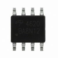
AO4620 Alpha & Omega Semiconductor Inc, AO4620 Datasheet

AO4620
Specifications of AO4620
Available stocks
Related parts for AO4620
AO4620 Summary of contents
Page 1
... AO4620 Complementary Enhancement Mode Field Effect Transistor General Description The AO4620 uses advanced trench technology MOSFETs to provide excellent R charge. The complementary MOSFETs may be used in inverter and other applications. SOIC-8 Top View Bottom View Pin1 Absolute Maximum Ratings T Parameter Drain-Source Voltage Gate-Source Voltage T =25° ...
Page 2
... AO4620 N-CHANNEL Electrical Characteristics (T Symbol Parameter STATIC PARAMETERS BV Drain-Source Breakdown Voltage DSS I Zero Gate Voltage Drain Current DSS I Gate-Body leakage current GSS V Gate Threshold Voltage GS(th state drain current D(ON) R Static Drain-Source On-Resistance DS(ON) g Forward Transconductance FS V Diode Forward Voltage SD I Maximum Body-Diode Continuous Current ...
Page 3
... AO4620 P-CHANNEL Electrical Characteristics (T Symbol Parameter STATIC PARAMETERS BV Drain-Source Breakdown Voltage DSS I Zero Gate Voltage Drain Current DSS I Gate-Body leakage current GSS V Gate Threshold Voltage GS(th state drain current D(ON) R Static Drain-Source On-Resistance DS(ON) g Forward Transconductance FS V Diode Forward Voltage SD I Maximum Body-Diode Continuous Current ...
Page 4
... AO4620 N-CHANNEL TYPICAL ELECTRICAL AND THERMAL CHARACTERISTICS 30 5V 10V (Volts) DS Figure 1: On-Region Characteristics (A) D Figure 3: On-Resistance vs. Drain Current and Gate Voltage THIS PRODUCT HAS BEEN DESIGNED AND QUALIFIED FOR THE CONSUMER MARKET. APPLICATIONS OR USES AS CRITICAL COMPONENTS IN LIFE SUPPORT DEVICES OR SYSTEMS ARE NOT AUTHORIZED. AOS DOES NOT ASSUME ANY LIABILITY ARISING 20 OUT OF SUCH APPLICATIONS OR USES OF ITS PRODUCTS ...
Page 5
... AO4620 N-CHANNEL TYPICAL ELECTRICAL AND THERMAL CHARACTERISTICS 10 V =15V DS I =7. (nC) g Figure 7: Gate-Charge Characteristics 100.0 10.0 R DS(ON) limited 1.0 T =150°C J(Max) 0.1 T =25°C A 0.0 0.01 0 (Volts) DS Figure 9: Maximum Forward Biased Safe Operating Area (Note =100°C THIS PRODUCT HAS BEEN DESIGNED AND QUALIFIED FOR THE CONSUMER MARKET. APPLICATIONS OR USES AS CRITICAL COMPONENTS IN LIFE SUPPORT DEVICES OR SYSTEMS ARE NOT AUTHORIZED ...
Page 6
... AO4620 P-CHANNEL TYPICAL ELECTRICAL AND THERMAL CHARACTERISTICS 30 -4.5V -10V 25 - (Volts) DS Figure 1: On-Region Characteristics 60 V =-4. (A) D Figure 3: On-Resistance vs. Drain Current and Gate Voltage Figure 5: On-Resistance vs. Gate-Source Voltage Alpha & Omega Semiconductor, Ltd - -3. =- 2.00 1.80 1.60 1.40 1.20 V =-10V 1.00 GS 0.80 - 1.0E+01 1.0E+00 I =-5 ...
Page 7
... AO4620 P-CHANNEL TYPICAL ELECTRICAL AND THERMAL CHARACTERISTICS 10 V =-15V DS I =-5. (nC) g Figure 7: Gate-Charge Characteristics 100.0 10.0 R DS(ON) limited 0.1s 1.0 10s 0.1 T =150°C J(Max) T =25°C A 0.0 0.01 0 (Volts) DS Figure 9: Maximum Forward Biased Safe Operating Area (Note =100°C/W ...


