IRF1010ESTRLPBF International Rectifier, IRF1010ESTRLPBF Datasheet
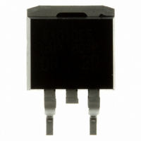
MOSFET N-CH 60V 84A D2PAK

IRF1010ESTRLPBF

Manufacturer Part Number
IRF1010ESTRLPBF
Description
MOSFET N-CH 60V 84A D2PAK
Manufacturer
International Rectifier
Series
HEXFET®r
Datasheets

Specifications of IRF1010ESTRLPBF

Fet Type
MOSFET N-Channel, Metal Oxide
Fet Feature
Standard
Rds On (max) @ Id, Vgs
12 mOhm @ 50A, 10V
Drain To Source Voltage (vdss)
60V
Current - Continuous Drain (id) @ 25° C
84A
Vgs(th) (max) @ Id
4V @ 250µA
Gate Charge (qg) @ Vgs
130nC @ 10V
Input Capacitance (ciss) @ Vds
3210pF @ 25V
Power - Max
200W
Mounting Type
Surface Mount
Package / Case
D²Pak, TO-263 (2 leads + tab)
Transistor Polarity
N Channel
Continuous Drain Current Id
84A
Drain Source Voltage Vds
60V
On Resistance Rds(on)
12mohm
Rds(on) Test Voltage Vgs
10V
Peak Reflow Compatible (260 C)
Yes
Rohs Compliant
Yes
Drain-source Breakdown Voltage
60 V
Gate-source Breakdown Voltage
20 V
Continuous Drain Current
83 A
Power Dissipation
170 W
Mounting Style
SMD/SMT
Gate Charge Qg
86.6 nC
Lead Free Status / RoHS Status
Lead free / RoHS Compliant
Other names
IRF1010ESTRLPBF
IRF1010ESTRLPBFTR

Available stocks

Company
Part Number
Manufacturer
Quantity
Price
Part Number:
IRF1010ESTRLPBF
Manufacturer:
International Rectifier
Quantity:
38 871
Part Number:
IRF1010ESTRLPBF
Manufacturer:
IR
Quantity:
20 000
Company:
Part Number:
IRF1010ESTRLPBF
Quantity:
9 000
l
l
l
l
l
l
l
Description
Absolute Maximum Ratings
Thermal Resistance
Advanced HEXFET
Rectifier utilize advanced processing techniques to
achieve extremely low on-resistance per silicon area.
This benefit, combined with the fast switching speed and
ruggedized device design that HEXFET power MOSFETs
are well known for, provides the designer with an
extremely efficient and reliable device for use in a wide
variety of applications.
The D
accommodating die sizes up to HEX-4. It provides the
highest power capability and the lowest possible on-
resistance in any existing surface mount package. The
D
low internal connection resistance and can dissipate up to
2.0W in a typical surface mount application.
The through-hole version (IRF1010EL) is available for low-
profile applications.
www.irf.com
I
I
I
P
V
I
E
dv/dt
T
T
R
R
D
D
DM
AR
2
J
STG
D
GS
AR
θJC
θJA
Pak is suitable for high current applications because of its
@ T
@ T
Advanced Process Technology
Surface Mount (IRF1010ES)
Low-profile through-hole (IRF1010EL)
175°C Operating Temperature
Fast Switching
Fully Avalanche Rated
Lead-Free
@T
2
C
C
C
Pak is a surface mount power package capable of
= 25°C
= 100°C
= 25°C
®
Continuous Drain Current, V
Pulsed Drain Current
Power Dissipation
Linear Derating Factor
Gate-to-Source Voltage
Avalanche Current
Repetitive Avalanche Energy
Peak Diode Recovery dv/dt
Operating Junction and
Storage Temperature Range
Soldering Temperature, for 10 seconds
Mounting torque, 6-32 or M3 srew
Junction-to-Case
Junction-to-Ambient (PCB mount)**
Power MOSFETs from International
Parameter
Parameter


ƒ
GS
GS

@ 10V
@ 10V
G
Typ.
300 (1.6mm from case )
–––
–––
10 lbf•in (1.1N•m)
HEXFET
-55 to + 175
IRF1010ES
S
D
IRF1010ESPbF
IRF1010ELPbF
D
Max.
84
330
200
± 20
1.4
4.0
59
50
17
2
Pak
®
R
Power MOSFET
DS(on)
Max.
V
0.75
I
40
D
DSS
= 84A‡
IRF1010EL
TO-262
PD - 95444
= 60V
= 12mΩ
Units
Units
°C/W
W/°C
V/ns
mJ
°C
W
A
V
A
1

Related parts for IRF1010ESTRLPBF

IRF1010ESTRLPBF Summary of contents

Page 1

Advanced Process Technology l l Surface Mount (IRF1010ES) l Low-profile through-hole (IRF1010EL) 175°C Operating Temperature l l Fast Switching Fully Avalanche Rated l Lead-Free l Description ® Advanced HEXFET Power MOSFETs from International Rectifier utilize advanced processing techniques to achieve ...

Page 2

Electrical Characteristics @ T Parameter V Drain-to-Source Breakdown Voltage (BR)DSS ∆V Breakdown Voltage Temp. Coefficient /∆T (BR)DSS J R Static Drain-to-Source On-Resistance DS(on) V Gate Threshold Voltage GS(th) g Forward Transconductance fs I Drain-to-Source Leakage Current DSS Gate-to-Source Forward Leakage ...

Page 3

VGS TOP 15V 10V 8.0V 7.0V 6.0V 5.5V 5.0V BOTTOM 4.5V 100 4.5V 10 20µs PULSE WIDTH 0 Drain-to-Source Voltage (V) DS Fig 1. Typical Output Characteristics 1000 T = ...

Page 4

0V MHZ C iss = rss = C gd 5000 C oss = Ciss 4000 3000 Coss 2000 Crss ...

Page 5

LIMITED BY PACKAGE 100 125 T , Case Temperature ( C) C Fig 9. Maximum Drain Current Vs. Case Temperature 0.50 0.20 0.1 0.10 0.05 SINGLE PULSE 0.02 ...

Page 6

D.U 20V V GS 0.01 Ω Charge 6 800 15V DRIVER 600 + 400 ...

Page 7

D.U.T + ‚ -  Driver Gate Drive D.U.T. I Reverse Recovery Current D.U.T. V Re-Applied Voltage Inductor Curent www.irf.com + • • ƒ • • • • Period D = P.W. Waveform SD Body Diode Forward Current ...

Page 8

Dimensions are shown in millimeters (inches HIS IS AN IRF530S WIT H LOT CODE 8024 AS S EMBLED ON WW 02, 2000 EMBLY LINE "L" Note: "P" sembly line pos ...

Page 9

TO-262 Package Outline Dimensions are shown in millimeters (inches) TO-262 Part Marking Information EXAMPLE: T HIS IS AN IRL 3103L LOT CODE 1789 AS S EMB LED ON WW 19, 1997 EMB LY LINE "C" ...

Page 10

Dimensions are shown in millimeters (inches) TRR FEED DIRECTION 1.85 (.073) 1.65 (.065) TRL FEED DIRECTION 330.00 (14.173) MAX. NOTES : 1. COMFORMS TO EIA-418. 2. CONTROLLING DIMENSION: MILLIMETER. 3. DIMENSION MEASURED @ HUB. 4. INCLUDES FLANGE DISTORTION @ ...

Page 11

Note: For the most current drawings please refer to the IR website at: http://www.irf.com/package/ ...

Related keywords