AO7401 Alpha & Omega Semiconductor Inc, AO7401 Datasheet - Page 2
AO7401
Manufacturer Part Number
AO7401
Description
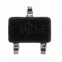
MOSFET P-CH -30V -1.2A SC70-3
Manufacturer
Alpha & Omega Semiconductor Inc
Datasheet
1.AO7401.pdf
(4 pages)
Specifications of AO7401
Fet Type
MOSFET P-Channel, Metal Oxide
Fet Feature
Logic Level Gate
Rds On (max) @ Id, Vgs
150 mOhm @ 1.2A, 10V
Drain To Source Voltage (vdss)
30V
Current - Continuous Drain (id) @ 25° C
1.2A
Vgs(th) (max) @ Id
1.4V @ 250µA
Gate Charge (qg) @ Vgs
5.06nC @ 4.5V
Input Capacitance (ciss) @ Vds
409pF @ 15V
Power - Max
350mW
Mounting Type
Surface Mount
Package / Case
SC-70-3, SOT-323-3
Lead Free Status / RoHS Status
Lead free / RoHS Compliant
Other names
785-1085-2
Available stocks
Company
Part Number
Manufacturer
Quantity
Price

Company:
Part Number:
AO7401
Manufacturer:
DIODES
Quantity:
1 655
Part Number:
AO7401
Manufacturer:
ALPHA
Quantity:
20 000
Company:
Part Number:
AO7401L
Manufacturer:
ALPHA
Quantity:
9 000
Part Number:
AO7401L
Manufacturer:
ALPHA
Quantity:
20 000


AO7401
Alpha & Omega Semiconductor, Ltd.
Electrical Characteristics (T
Symbol
STATIC PARAMETERS
BV
I
I
V
I
R
g
V
I
DYNAMIC PARAMETERS
C
C
C
R
SWITCHING PARAMETERS
Q
Q
Q
t
t
t
t
t
Q
A: The value of R
value in any given application depends on the user's specific board design. The current rating is based on the t ≤ 10s thermal resistance rating.
B: Repetitive rating, pulse width limited by junction temperature.
C. The R
D. The static characteristics in Figures 1 to 6,12,14 are obtained using <300 µs pulses, duty cycle 0.5% max.
E. These tests are performed with the device mounted on 1 in
curve provides a single pulse rating.
Rev 5 : Aug 2008
THIS PRODUCT HAS BEEN DESIGNED AND QUALIFIED FOR THE CONSUMER MARKET. APPLICATIONS OR USES AS CRITICAL
COMPONENTS IN LIFE SUPPORT DEVICES OR SYSTEMS ARE NOT AUTHORIZED. AOS DOES NOT ASSUME ANY LIABILITY ARISING
OUT OF SUCH APPLICATIONS OR USES OF ITS PRODUCTS. AOS RESERVES THE RIGHT TO IMPROVE PRODUCT DESIGN,
FUNCTIONS AND RELIABILITY WITHOUT NOTICE.
DSS
GSS
D(ON)
S
D(on)
r
D(off)
f
rr
FS
GS(th)
SD
DS(ON)
iss
oss
rss
g
g
gs
gd
rr
DSS
θJA
is the sum of the thermal impedence from junction to lead R
Drain-Source Breakdown Voltage
Zero Gate Voltage Drain Current
Gate-Body leakage current
Gate Threshold Voltage
On state drain current
Static Drain-Source On-Resistance
Forward Transconductance
Diode Forward Voltage
Maximum Body-Diode Continuous Current
Input Capacitance
Output Capacitance
Reverse Transfer Capacitance
Gate resistance
Total Gate Charge
Gate Source Charge
Gate Drain Charge
Turn-On DelayTime
Turn-On Rise Time
Turn-Off DelayTime
Turn-Off Fall Time
Body Diode Reverse Recovery Time
Body Diode Reverse Recovery Charge
θJA
is measured with the device mounted on 1in
Parameter
J
=25°C unless otherwise noted)
2
FR-4 board with 2oz. Copper, in a still air environment with T
2
Conditions
I
V
V
V
V
V
V
V
V
I
V
V
V
V
R
I
I
FR-4 board with 2oz. Copper, in a still air environment with T
D
S
F
F
DS
DS
DS
GS
GS
GS
GS
DS
GS
GS
GS
GS
=-1A, dI/dt=100A/µs
=-1A, dI/dt=100A/µs
=-250µA, V
=-1A,V
GEN
=-24V, V
=0V, V
=V
=-4.5V, V
=-10V, I
=-4.5V, I
=-2.5V, I
=-5V, I
=0V, V
=0V, V
=-4.5V, V
=-10V, V
θJL
=3Ω
GS
and lead to ambient.
GS
I
D
D
GS
DS
DS
=0V
=-250µA
=-1.2A
D
D
D
GS
=±12V
=-15V, f=1MHz
=0V, f=1MHz
DS
=-1.2A
GS
DS
DS
=-1.2A
=-1A
=0V
=-15V, R
=0V
=-5V
=-15V, I
D
T
L
=-1A
=15Ω,
T
J
=125°C
J
=55°C
Min
-0.6
-30
-10
3
-0.85
5.06
0.72
1.58
41.2
14.5
13.2
Typ
122
173
147
207
409
4.5
6.2
3.2
5.4
55
42
12
-1
A
=25°C. The SOA
A
=25°C. The
±100
Max
-1.4
-0.5
150
220
200
280
-1
-5
-1
Units
mΩ
mΩ
mΩ
µA
nA
nC
nC
nC
nC
pF
pF
pF
ns
ns
ns
ns
ns
Ω
V
V
A
S
V
A
Related parts for AO7401
Image
Part Number
Description
Manufacturer
Datasheet
Request
R

Part Number:
Description:
MOSFET DUAL N-CH 40V 6A 8-SOIC
Manufacturer:
Alpha & Omega Semiconductor Inc
Datasheet:

Part Number:
Description:
MOSFET DUAL N-CH 30V 6.9A 8-SOIC
Manufacturer:
Alpha & Omega Semiconductor Inc
Datasheet:

Part Number:
Description:
MOSFET DUAL P-CH -30V -6A 8-SOIC
Manufacturer:
Alpha & Omega Semiconductor Inc
Datasheet:

Part Number:
Description:
MOSFET DUAL N-CH 30V 9A ASYM SO8
Manufacturer:
Alpha & Omega Semiconductor Inc
Datasheet:

Part Number:
Description:
MOSFET DUAL PCH -30V -7.1A 8SOIC
Manufacturer:
Alpha & Omega Semiconductor Inc
Datasheet:

Part Number:
Description:
MOSFET DUAL P-CH -12V -7A 8TSSOP
Manufacturer:
Alpha & Omega Semiconductor Inc
Datasheet:

Part Number:
Description:
MOSFET N/P-CH COMPL 20V 6-TSOP
Manufacturer:
Alpha & Omega Semiconductor Inc
Datasheet:

Part Number:
Description:
MOSFET N/P-CH COMPL 20V 8-SOIC
Manufacturer:
Alpha & Omega Semiconductor Inc
Datasheet:

Part Number:
Description:
MOSFET N/P-CH COMPL 60V 8-PDIP
Manufacturer:
Alpha & Omega Semiconductor Inc
Datasheet:

Part Number:
Description:
MOSFET N/P-CH COMPL 30V 8-PDIP
Manufacturer:
Alpha & Omega Semiconductor Inc
Datasheet:

Part Number:
Description:
MOSFET DUAL N-CH 20V 9.4A 8-SOIC
Manufacturer:
Alpha & Omega Semiconductor Inc
Datasheet:

Part Number:
Description:
MOSFET DUAL N-CH 30V 3.4A 6-TSOP
Manufacturer:
Alpha & Omega Semiconductor Inc
Datasheet:

Part Number:
Description:
MOSFET DUAL N-CH 60V 4.5A 8-SOIC
Manufacturer:
Alpha & Omega Semiconductor Inc
Datasheet:

Part Number:
Description:
MOSFET N/P-CH COMPL 60V 8-SOIC
Manufacturer:
Alpha & Omega Semiconductor Inc
Datasheet:

Part Number:
Description:
MOSFET P-CH 20V 0.6A SC70-6
Manufacturer:
Alpha & Omega Semiconductor Inc
Datasheet: