AO3423 Alpha & Omega Semiconductor Inc, AO3423 Datasheet
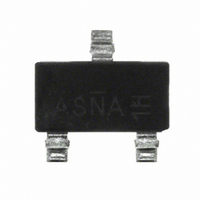
MOSFET P-CH -20V -2A SOT23

AO3423

Manufacturer Part Number
AO3423
Description
MOSFET P-CH -20V -2A SOT23
Manufacturer
Alpha & Omega Semiconductor Inc
Datasheet

Specifications of AO3423

Fet Type
MOSFET P-Channel, Metal Oxide
Fet Feature
Logic Level Gate
Rds On (max) @ Id, Vgs
92 mOhm @ 2A, 10V
Drain To Source Voltage (vdss)
20V
Current - Continuous Drain (id) @ 25° C
2A
Vgs(th) (max) @ Id
1.4V @ 250µA
Gate Charge (qg) @ Vgs
6.6nC @ 4.5V
Input Capacitance (ciss) @ Vds
620pF @ 10V
Power - Max
1.4W
Mounting Type
Surface Mount
Package / Case
SOT-23-3, TO-236-3, Micro3™, SSD3, SST3
Lead Free Status / RoHS Status
Lead free / RoHS Compliant
Other names
785-1016-2

Available stocks

Company
Part Number
Manufacturer
Quantity
Price
Part Number:
AO3423
Manufacturer:
Alpha
Quantity:
13 500
Part Number:
AO3423
Manufacturer:
AOS
Quantity:
2 799
Part Number:
AO3423
Manufacturer:
AOS/万代
Quantity:
20 000
Part Number:
AO3423/AS
Manufacturer:
AO
Quantity:
20 000
Part Number:
AO3423A
Manufacturer:
AOS/ 万代
Quantity:
20 000
Alpha & Omega Semiconductor, Ltd.
Absolute Maximum Ratings T
Parameter
Drain-Source Voltage
Gate-Source Voltage
Continuous Drain
Current
Pulsed Drain Current
Power Dissipation
Junction and Storage Temperature Range
Thermal Characteristics
Parameter
Maximum Junction-to-Ambient
Maximum Junction-to-Lead
General Description
The AO3423/L uses advanced trench technology to
provide excellent R
operation with gate voltages as low as 2.5V. This
device is suitable for use as a load switch or in PWM
applications. It is ESD protected.AO3423 and
AO3423L are electrically identical.
-RoHS Compliant
-AO3423L is Halogen Free
AO3423
P-Channel Enhancement Mode Field Effect Transistor
A
A
DS(ON)
G
S
B
T
T
T
T
A
A
A
A
(SOT-23)
Top View
=25°C
=70°C
=25°C
=70°C
TO-236
, low gate charge and
C
A
A
F
F
A
D
=25°C unless otherwise noted
Steady-State
Steady-State
t ≤ 10s
Symbol
V
V
I
I
P
T
D
DM
J
DS
GS
D
, T
STG
Symbol
Features
V
I
R
R
R
ESD Rating: 2000V HBM
R
D
R
DS
DS(ON)
DS(ON)
DS(ON)
θJA
θJL
= -2 A
(V) = -20V
G
< 92mΩ (V
< 118mΩ (V
< 166mΩ (V
Maximum
-55 to 150
Typ
±12
1.4
0.9
-20
-2
-2
65
85
43
-8
D
S
(V
GS
GS
GS
GS
= -10V)
= -10V)
= -4.5V)
= -2.5V)
Max
125
90
60
Units
Units
°C/W
°C/W
°C/W
°C
W
V
V
A

Related parts for AO3423

AO3423 Summary of contents

Page 1

... AO3423 P-Channel Enhancement Mode Field Effect Transistor General Description The AO3423/L uses advanced trench technology to provide excellent R , low gate charge and DS(ON) operation with gate voltages as low as 2.5V. This device is suitable for use as a load switch or in PWM applications ESD protected.AO3423 and AO3423L are electrically identical ...

Page 2

... AO3423 Electrical Characteristics (T =25°C unless otherwise noted) J Parameter Symbol STATIC PARAMETERS BV Drain-Source Breakdown Voltage DSS I Zero Gate Voltage Drain Current DSS I Gate-Body leakage current GSS V Gate Threshold Voltage GS(th state drain current D(ON) R Static Drain-Source On-Resistance DS(ON) g Forward Transconductance FS V Diode Forward Voltage ...

Page 3

... AO3423 TYPICAL ELECTRICAL AND THERMAL CHARACTERISTICS 15 -10.0V -4.0V -8.0V -3.5V 12 -6. (Volts) DS Fig 1: On-Region Characteristics 180 V =-2.5V GS 160 140 V =-4.5V GS 120 100 (A) D Figure 3: On-Resistance vs. Drain Current and Gate Voltage 200 180 160 140 120 100 80 25° (Volts) GS Figure 5: On-Resistance vs. Gate-Source Voltage Alpha & ...

Page 4

... AO3423 TYPICAL ELECTRICAL AND THERMAL CHARACTERISTICS (nC) g Figure 7: Gate-Charge Characteristics 10.0 R DS(ON) limited 1.0 1s 10s T =150°C DC J(Max) T =25°C A 0.1 0 (Volts) DS Figure 9: Maximum Forward Biased Safe Operating Area (Note θJA θJA J, =90°C/W θJA 1 0.1 Single Pulse 0.01 ...

Related keywords