SI4401BDY-T1-E3 Vishay, SI4401BDY-T1-E3 Datasheet - Page 2
SI4401BDY-T1-E3
Manufacturer Part Number
SI4401BDY-T1-E3
Description
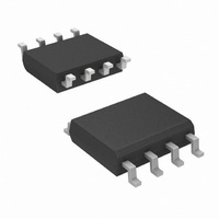
MOSFET P-CH 40V 8.7A 8-SOIC
Manufacturer
Vishay
Series
TrenchFET®r
Datasheet
1.SI4401BDY-T1-GE3.pdf
(6 pages)
Specifications of SI4401BDY-T1-E3
Transistor Polarity
P-Channel
Fet Type
MOSFET P-Channel, Metal Oxide
Fet Feature
Logic Level Gate
Rds On (max) @ Id, Vgs
14 mOhm @ 10.5A, 10V
Drain To Source Voltage (vdss)
40V
Current - Continuous Drain (id) @ 25° C
8.7A
Vgs(th) (max) @ Id
3V @ 250µA
Gate Charge (qg) @ Vgs
55nC @ 5V
Power - Max
1.5W
Mounting Type
Surface Mount
Package / Case
8-SOIC (3.9mm Width)
Minimum Operating Temperature
- 55 C
Configuration
Single Quad Drain Triple Source
Resistance Drain-source Rds (on)
0.014 Ohm @ 10 V
Drain-source Breakdown Voltage
40 V
Gate-source Breakdown Voltage
+/- 20 V
Continuous Drain Current
8.7 A
Power Dissipation
1500 mW
Maximum Operating Temperature
+ 150 C
Mounting Style
SMD/SMT
Continuous Drain Current Id
-8.7A
Drain Source Voltage Vds
-40V
On Resistance Rds(on)
21mohm
Rds(on) Test Voltage Vgs
-4.5V
Threshold Voltage Vgs Typ
-3V
Lead Free Status / RoHS Status
Lead free / RoHS Compliant
Lead Free Status / RoHS Status
Lead free / RoHS Compliant, Lead free / RoHS Compliant
Other names
SI4401BDY-T1-E3TR
Available stocks
Company
Part Number
Manufacturer
Quantity
Price
Company:

Part Number:
SI4401BDY-T1-E3
Manufacturer:
Vishay/Siliconix
Quantity:
24 887
Company:
Part Number:
SI4401BDY-T1-E3
Manufacturer:
NICCOMPHIA
Quantity:
30 000
Company:
Part Number:
SI4401BDY-T1-E3
Manufacturer:
VISHAY
Quantity:
15 000
Part Number:
SI4401BDY-T1-E3
Manufacturer:
VISHAY/威世
Quantity:
20 000


Si4401BDY
Vishay Siliconix
Notes:
a. Pulse test; pulse width ≤ 300 µs, duty cycle ≤ 2 %.
b. Guaranteed by design, not subject to production testing.
Stresses beyond those listed under “Absolute Maximum Ratings” may cause permanent damage to the device. These are stress ratings only, and functional operation
of the device at these or any other conditions beyond those indicated in the operational sections of the specifications is not implied. Exposure to absolute maximum
rating conditions for extended periods may affect device reliability.
TYPICAL CHARACTERISTICS 25 °C, unless otherwise noted
www.vishay.com
2
SPECIFICATIONS T
Parameter
Static
Gate Threshold Voltage
Gate-Body Leakage
Zero Gate Voltage Drain Current
On-State Drain Current
Drain-Source On-State Resistance
Forward Transconductance
Diode Forward Voltage
Dynamic
Total Gate Charge
Gate-Source Charge
Gate-Drain Charge
Gate Resistance
Turn-On Delay Time
Rise Time
Turn-Off Delay Time
Fall Time
Source-Drain Reverse Recovery Time
b
50
40
30
20
10
0
0
1
a
a
V
DS
Output Characteristics
a
- Drain-to-Source Voltage (V)
J
V
= 25 °C, unless otherwise noted
GS
2
= 10 V thru 4 V
a
Symbol
R
V
3
I
t
t
I
I
DS(on)
GS(th)
D(on)
V
Q
Q
d(on)
d(off)
GSS
DSS
Q
g
R
t
t
t
SD
rr
fs
gs
gd
r
f
g
g
4
V
DS
V
3 V
I
D
DS
≅ - 1 A, V
= - 15 V, V
I
F
= - 40 V, V
V
V
V
V
V
V
V
V
= - 2.1 A, dI/dt = 100 A/µs
GS
DS
DS
GS
I
DS
5
DS
S
DD
DS
= - 2.7 A, V
Test Conditions
= - 10 V, I
= - 15 V, I
= V
= - 4.5 V, I
= - 5 V, V
= 0 V, V
= - 40 V, V
= - 15 V, R
GEN
GS
GS
GS
, I
= - 5 V, I
= - 10 V, R
D
GS
= 0 V, T
GS
D
D
= - 250 µA
D
GS
= - 10.5 A
= - 10.5 A
GS
L
= ± 20 V
= - 8.7 A
= - 10 V
= 15 Ω
= 0 V
= 0 V
D
J
= - 10.5 A
= 70 °C
g
= 6 Ω
50
40
30
20
10
0
0.0
0.5
Min.
- 1.0
- 30
1.4
1.0
V
Transfer Characteristics
GS
- Gate-to-Source Voltage (V)
1.5
T
25 °C
0.0165
C
0.011
- 0.74
Typ.
2.0
2.8
= 125 °C
26
40
10
14
16
15
97
47
35
S09-0866-Rev. D, 18-May-09
Document Number: 73140
2.5
± 100
0.014
0.021
3.0
Max.
- 3.0
- 1.1
- 10
150
4.2
- 1
55
25
25
75
55
- 55 °C
3.5
4.0
Unit
nC
nA
µA
ns
Ω
Ω
V
A
S
V
4.5
Related parts for SI4401BDY-T1-E3
Image
Part Number
Description
Manufacturer
Datasheet
Request
R

Part Number:
Description:
P-channel 40-v D-s Mosfet
Manufacturer:
Vishay
Datasheet:

Part Number:
Description:
MOSFET P-CH 40V 8.7A 8-SOIC
Manufacturer:
Vishay
Datasheet:

Part Number:
Description:
357-036-542-201 CARDEDGE 36POS DL .156 BLK LOPRO
Manufacturer:
Vishay
Datasheet:
Part Number:
Description:
357-036-542-201 CARDEDGE 36POS DL .156 BLK LOPRO
Manufacturer:
Vishay
Datasheet:
Part Number:
Description:
357-036-542-201 CARDEDGE 36POS DL .156 BLK LOPRO
Manufacturer:
Vishay
Datasheet:
Part Number:
Description:
357-036-542-201 CARDEDGE 36POS DL .156 BLK LOPRO
Manufacturer:
Vishay
Datasheet:
Part Number:
Description:
357-036-542-201 CARDEDGE 36POS DL .156 BLK LOPRO
Manufacturer:
Vishay
Datasheet:
Part Number:
Description:
357-036-542-201 CARDEDGE 36POS DL .156 BLK LOPRO
Manufacturer:
Vishay
Datasheet:
Part Number:
Description:
357-036-542-201 CARDEDGE 36POS DL .156 BLK LOPRO
Manufacturer:
Vishay
Datasheet:
Part Number:
Description:
357-036-542-201 CARDEDGE 36POS DL .156 BLK LOPRO
Manufacturer:
Vishay
Datasheet:
Part Number:
Description:
357-036-542-201 CARDEDGE 36POS DL .156 BLK LOPRO
Manufacturer:
Vishay
Datasheet:
Part Number:
Description:
357-036-542-201 CARDEDGE 36POS DL .156 BLK LOPRO
Manufacturer:
Vishay
Datasheet:
Part Number:
Description:
357-036-542-201 CARDEDGE 36POS DL .156 BLK LOPRO
Manufacturer:
Vishay
Datasheet: