IRFP250MPBF International Rectifier, IRFP250MPBF Datasheet - Page 2
IRFP250MPBF
Manufacturer Part Number
IRFP250MPBF
Description
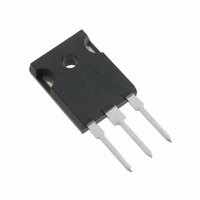
MOSFET N-CH 200V 30A TO-247AC
Manufacturer
International Rectifier
Series
HEXFET®r
Datasheet
1.IRFP250MPBF.pdf
(8 pages)
Specifications of IRFP250MPBF
Fet Type
MOSFET N-Channel, Metal Oxide
Fet Feature
Standard
Rds On (max) @ Id, Vgs
75 mOhm @ 18A, 10V
Drain To Source Voltage (vdss)
200V
Current - Continuous Drain (id) @ 25° C
30A
Vgs(th) (max) @ Id
4V @ 250µA
Gate Charge (qg) @ Vgs
123nC @ 10V
Input Capacitance (ciss) @ Vds
2159pF @ 25V
Power - Max
214W
Mounting Type
Through Hole
Package / Case
TO-247-3 (Straight Leads), TO-247AC
Transistor Polarity
N Channel
Continuous Drain Current Id
30A
Drain Source Voltage Vds
200V
On Resistance Rds(on)
75mohm
Rds(on) Test Voltage Vgs
10V
Threshold Voltage Vgs Typ
4V
Rohs Compliant
Yes
Drain-source Breakdown Voltage
200 V
Gate-source Breakdown Voltage
20 V
Continuous Drain Current
30 A
Power Dissipation
214 W
Mounting Style
Through Hole
Gate Charge Qg
82 nC
Lead Free Status / RoHS Status
Lead free / RoHS Compliant
Available stocks
Company
Part Number
Manufacturer
Quantity
Price
Company:

Part Number:
IRFP250MPBF
Manufacturer:
FSC
Quantity:
9 000
Part Number:
IRFP250MPBF
Manufacturer:
IR
Quantity:
20 000


IRFP250MPbF
Source-Drain Ratings and Characteristics
Electrical Characteristics @ T
‚
Notes:
V
∆V
R
V
g
I
I
Q
Q
Q
t
t
t
t
C
C
C
L
L
I
I
V
t
Q
t
DSS
GSS
SM
d(on)
r
d(off)
f
S
rr
on
fs
D
S
(BR)DSS
GS(th)
SD
2
DS(on)
g
gs
gd
iss
oss
rss
rr
Repetitive rating; pulse width limited by
(BR)DSS
max. junction temperature. (See Fig. 11)
R
Starting T
G
= 25Ω, I
/∆T
J
J
Drain-to-Source Leakage Current
Drain-to-Source Breakdown Voltage
Breakdown Voltage Temp. Coefficient
Static Drain-to-Source On-Resistance
Gate Threshold Voltage
Forward Transconductance
Gate-to-Source Forward Leakage
Gate-to-Source Reverse Leakage
Total Gate Charge
Gate-to-Source Charge
Gate-to-Drain ("Miller") Charge
Turn-On Delay Time
Rise Time
Turn-Off Delay Time
Fall Time
Input Capacitance
Output Capacitance
Reverse Transfer Capacitance
Continuous Source Current
(Body Diode)
Pulsed Source Current
(Body Diode)
Diode Forward Voltage
Reverse Recovery Time
Reverse Recovery Charge
Forward Turn-On Time
Internal Drain Inductance
Internal Source Inductance
= 25°C, L = 1.9mH
AS
= 18A. (See Figure 12)
Parameter
Parameter
J
= 25°C (unless otherwise specified)
ƒ
„
Pulse width ≤ 300µs; duty cycle ≤ 2%.
T
200
–––
–––
–––
–––
–––
–––
–––
–––
–––
–––
–––
–––
–––
–––
–––
–––
–––
Min. Typ. Max. Units
2.0
Min. Typ. Max. Units
17
–––
–––
–––
–––
–––
–––
J
≤ 175°C
Intrinsic turn-on time is negligible (turn-on is dominated by L
≤ 18A di/d ≤ 374A/µs, V
2159 –––
0.26
–––
–––
–––
–––
–––
–––
––– -100
–––
–––
–––
315
––– 0.075
–––
–––
–––
186
1.3
4.5
83
14
43
41
33
7.5
–––
–––
–––
–––
250
100
123
–––
–––
–––
–––
–––
–––
–––
120
279
4.0
1.3
2.0
25
21
57
30
V/°C
µA
nA
nC
ns
µC
pF
ns
nH
Ω
V
V
S
A
V
V
Reference to 25°C, I
V
V
V
V
V
V
V
I
V
V
V
I
R
R
Between lead,
6mm (0.25in.)
from package
and center of die contact
V
V
ƒ = 1.0MHz, See Fig. 5
MOSFET symbol
showing the
integral reverse
p-n junction diode.
T
T
di/dt = 100A/µs
D
D
DD
GS
GS
DS
DS
DS
DS
GS
GS
DS
GS
DD
GS
DS
J
J
G
D
= 18A
= 18A
= 25°C, I
= 25°C, I
= 5.5Ω, See Fig. 10 „
= 3.9Ω
≤ V
= 0V, I
= 10V, I
= V
= 50V, I
= 200V, V
= 160V, V
= 20V
= -20V
= 160V
= 10V, See Fig. 6 and 13
= 100V
= 0V
= 25V
(BR)DSS
GS
, I
D
S
F
D
D
D
Conditions
= 250µA
Conditions
= 18A
= 18A, V
,
= 18A
= 250µA
= 18A „
GS
GS
„
= 0V
= 0V, T
D
GS
= 1mA
„
www.irf.com
J
= 0V
G
= 150°C
G
S
„
+L
„
D
S
D
)
S
D
Related parts for IRFP250MPBF
Image
Part Number
Description
Manufacturer
Datasheet
Request
R

Part Number:
Description:
SCHOTTKY RECTIFIER
Manufacturer:
International Rectifier Corp.
Datasheet:
Part Number:
Description:
SCHOTTKY RECTIFIER
Manufacturer:
International Rectifier Corp.
Datasheet:
Part Number:
Description:
SCHOTTKY RECTIFIER
Manufacturer:
International Rectifier Corp.
Datasheet:
Part Number:
Description:
SCHOTTKY RECTIFIER
Manufacturer:
International Rectifier Corp.
Datasheet:
Part Number:
Description:
SCHOTTKY RECTIFIER
Manufacturer:
International Rectifier Corp.
Datasheet:
Part Number:
Description:
SCHOTTKY RECTIFIER
Manufacturer:
International Rectifier Corp.
Datasheet:
Part Number:
Description:
SCHOTTKY RECTIFIER
Manufacturer:
International Rectifier Corp.
Datasheet:
Part Number:
Description:
SCHOTTKY RECTIFIER
Manufacturer:
International Rectifier Corp.
Datasheet:
Part Number:
Description:
SCHOTTKY RECTIFIER
Manufacturer:
International Rectifier Corp.
Datasheet:
Part Number:
Description:
SCHOTTKY RECTIFIER
Manufacturer:
International Rectifier Corp.
Datasheet:
Part Number:
Description:
SCHOTTKY RECTIFIER
Manufacturer:
International Rectifier Corp.
Datasheet:
Part Number:
Description:
SCHOTTKY RECTIFIER
Manufacturer:
International Rectifier Corp.
Datasheet:
Part Number:
Description:
SCHOTTKY RECTIFIER
Manufacturer:
International Rectifier Corp.
Datasheet:
Part Number:
Description:
SCHOTTKY RECTIFIER
Manufacturer:
International Rectifier Corp.
Datasheet:
Part Number:
Description:
SCHOTTKY RECTIFIER
Manufacturer:
International Rectifier Corp.
Datasheet: