AO6701 Alpha & Omega Semiconductor Inc, AO6701 Datasheet
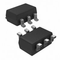
MOSFET P-CH -30V -2.3A 6-TSOP

AO6701

Manufacturer Part Number
AO6701
Description
MOSFET P-CH -30V -2.3A 6-TSOP
Manufacturer
Alpha & Omega Semiconductor Inc
Datasheet

Specifications of AO6701

Fet Type
MOSFET P-Channel, Metal Oxide
Fet Feature
Diode (Isolated)
Rds On (max) @ Id, Vgs
135 mOhm @ 2.3A, 10V
Drain To Source Voltage (vdss)
30V
Current - Continuous Drain (id) @ 25° C
2.3A
Vgs(th) (max) @ Id
1.4V @ 250µA
Gate Charge (qg) @ Vgs
4.9nC @ 4.5V
Input Capacitance (ciss) @ Vds
409pF @ 15V
Power - Max
1.15W
Mounting Type
Surface Mount
Package / Case
6-TSOP
Lead Free Status / RoHS Status
Lead free / RoHS Compliant
Other names
785-1079-2

Available stocks

Company
Part Number
Manufacturer
Quantity
Price
Part Number:
AO6701
Manufacturer:
ALPHA
Quantity:
33 000
Absolute Maximum Ratings T
Parameter
Drain-Source Voltage
Gate-Source Voltage
Continuous Drain Current
Pulsed Drain Current
Schottky reverse voltage
Continuous Forward Current
Pulsed Forward Current
Power Dissipation
Junction and Storage Temperature Range
Parameter: Thermal Characteristics MOSFET
Maximum Junction-to-Ambient
Maximum Junction-to-Lead
Thermal Characteristics Schottky
Maximum Junction-to-Ambient
Maximum Junction-to-Lead
AO6701
P-Channel Enhancement Mode Field Effect Transistor
with Schottky Diode
General Description
The AO6701 uses advanced trench technology to provide
excellent R
provided to facilitate the implementation of a bidirectional
blocking switch, or for DC-DC conversion applications.
Standard Product AO6701 is Pb-free (meets ROHS & Sony
259 specifications). AO6701L is a Green Product ordering
option. AO6701 and AO6701L are electrically identical.
A
S
G
TSOP6
DS(ON)
1
2
3
6
5
4
and low gate charge. A Schottky diode is
K
N/C
D
B
B
A
C
C
A
A
A
A
A
A
=25°C unless otherwise noted
Steady-State
Steady-State
Steady-State
Steady-State
t ≤ 10s
t ≤ 10s
T
T
T
T
T
T
A
A
A
A
A
A
=25°C
=70°C
=25°C
=70°C
=25°C
=70°C
G
Symbol
Symbol
T
D
S
J
R
R
R
R
V
V
V
, T
I
I
P
I
DM
I
FM
θJA
θJA
GS
θJL
θJL
DS
D
KA
F
D
STG
Features
V
I
R
R
R
SCHOTTKY
V
D
DS
DS
DS(ON)
DS(ON)
DS(ON)
= -2.3A (V
K
A
(V) = -30V
(V) = 20V, I
-55 to 150
MOSFET
< 135mΩ (V
< 185mΩ (V
< 265mΩ (V
109.4
136.5
1.15
58.5
Typ
±12
-2.3
-1.8
106
-30
-15
0.7
78
64
GS
F
= -10V)
= 1A, V
GS
GS
GS
= -10V)
= -4.5V)
= -2.5V)
-55 to 150
Schottky
F
<0.5V@0.5A
Max
0.92
0.59
110
150
135
175
20
10
80
80
2
1
Units
Units
°C/W
°C/W
°C
W
V
V
A
V
A

Related parts for AO6701

AO6701 Summary of contents

Page 1

... A Schottky diode is DS(ON) provided to facilitate the implementation of a bidirectional blocking switch, or for DC-DC conversion applications. Standard Product AO6701 is Pb-free (meets ROHS & Sony 259 specifications). AO6701L is a Green Product ordering option. AO6701 and AO6701L are electrically identical. A ...

Page 2

... AO6701 Electrical Characteristics (T =25°C unless otherwise noted) J Parameter Symbol STATIC PARAMETERS BV Drain-Source Breakdown Voltage DSS I Zero Gate Voltage Drain Current DSS I Gate-Body leakage current GSS V Gate Threshold Voltage GS(th state drain current D(ON) R Static Drain-Source On-Resistance DS(ON) g Forward Transconductance FS V Diode Forward Voltage ...

Page 3

... AO6701 MOSFET TYPICAL ELECTRICAL AND THERMAL CHARACTERISTICS 20 -10V (Volts) DS Fig 1: On-Region Characteristics 250 225 V GS 200 175 150 V =-4.5V GS 125 100 (A) D Figure 3: On-Resistance vs. Drain Current and Gate Voltage 350 300 250 200 150 100 (Volts) GS Figure 5: On-Resistance vs. Gate-Source Voltage Alpha & Omega Semiconductor, Ltd. ...

Page 4

... AO6701 MOSFET TYPICAL ELECTRICAL AND THERMAL CHARACTERISTICS 5 V =-15V DS I =-2. (nC) g Figure 7: Gate-Charge Characteristics 100.0 T =150°C J(Max) T =25°C A 10.0 100µs R DS(ON) limited 1ms 0.1s 10ms 1.0 1s 10s DC 0.1 0 (Volts) DS Figure 9: Maximum Forward Biased Safe Operating Area (Note E) 10 ...

Page 5

... AO6701 TYPICAL ELECTRICAL AND THERMAL CHARACTERISTICS: SCHOTTKY 1.0E+01 125°C 1.0E+00 1.0E-01 1.0E-02 25°C 1.0E-03 0.0 0.2 0.4 0.6 V (Volts) F Figure 12: Schottky Forward Characteristics 0.5 0.4 I =0.5A F 0.3 0.2 0 Temperature (°C) Figure 14: Schottky Forward Drop vs. Junction Temperature 10 D θJA J, =135°C/W θ ...

Related keywords