AOD403 Alpha & Omega Semiconductor Inc, AOD403 Datasheet
AOD403
Specifications of AOD403
Available stocks


Related parts for AOD403


AOD403 Summary of contents
Page 1
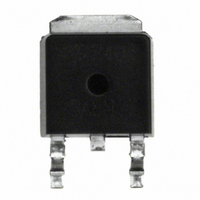
... General Description The AOD403/AOI403 uses advanced trench technology to provide excellent R , low gate charge and low gate DS(ON) resistance. With the excellent thermal resistance of the DPAK/IPAK package, this device is well suited for high current load applications. TO252 TO252 DPAK DPAK Top View ...
Page 2
... Ratings are based on low frequency and duty cycles to keep initial J(MAX) and case to ambient FR-4 board with 2oz. Copper still air environment with T www.aosmd.com AOD403/AOI403 Min Typ Max - =55° C ...
Page 3
... Figure 4: On-Resistance vs. Junction Temperature Figure 4: On-Resistance vs. Junction Temperature 1.0E+02 I =-20A D 1.0E+01 40 1.0E+00 125°C 1.0E-01 1.0E-02 1.0E-03 1.0E-04 1.0E- 0.0 Figure 6: Body-Diode Characteristics (Note E) www.aosmd.com AOD403/AOI403 125°C 125°C 25°C 25°C 2.5 2 3.5 3 4.5 4 5.5 5 (Volts) (Volts =-20V =-20V GS ...
Page 4
... Figure 10: Single Pulse Power Rating Junction-to- Figure 10: Single Pulse Power Rating Junction-to- In descending order D=0.5, 0.3, 0.1, 0.05, 0.02, 0.01, single pulse 40 0.001 0.01 0.1 Pulse Width (s) www.aosmd.com AOD403/AOI403 C C iss iss C C oss oss (Volts) (Volts) ...
Page 5
... Figure 15: Single Pulse Power Rating Junction-to- Figure 15: Single Pulse Power Rating Junction-to- In descending order D=0.5, 0.3, 0.1, 0.05, 0.02, 0.01, single pulse 40 Single Pulse 0.01 0.1 Pulse Width (s) www.aosmd.com AOD403/AOI403 100 100 125 125 150 150 175 175 ...
Page 6
... Vdd Vdd VDC VDC + + Vds Vds Vds Vds - Vgs Vdd VDC Id + Vgs Diode Recovery Test Circuit & Waveforms Vgs -Isd + Vdd VDC - -Vds www.aosmd.com AOD403/AOI403 Qg Qg Qgs Qgs Qgd Qgd Charge Charge t t off off d(off) d(off 90% 90% 10% 10 DSS ...