SI5326C-C-GM Silicon Laboratories Inc, SI5326C-C-GM Datasheet - Page 61
SI5326C-C-GM
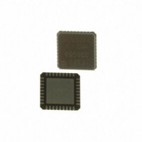
Manufacturer Part Number
SI5326C-C-GM
Description
DSPLL 36-Pin QFN EP
Manufacturer
Silicon Laboratories Inc
Type
Jitter Attenuatorr
Datasheet
1.SI5326B-C-GM.pdf
(72 pages)
Specifications of SI5326C-C-GM
Package
36QFN EP
Operating Temperature
-40 to 85 °C
Pll
Yes
Input
Clock
Output
CML, CMOS, LVDS, LVPECL
Number Of Circuits
1
Ratio - Input:output
2:2
Differential - Input:output
Yes/Yes
Frequency - Max
346MHz
Divider/multiplier
Yes/Yes
Voltage - Supply
1.71 V ~ 3.63 V
Mounting Type
Surface Mount
Package / Case
36-QFN
Frequency-max
346MHz
Operating Temperature (max)
85C
Operating Temperature (min)
-40C
Package Type
QFN EP
Mounting
Surface Mount
Lead Free Status / RoHS Status
Lead free / RoHS Compliant
Lead Free Status / RoHS Status
Lead free / RoHS Compliant
Other names
336-1746
336-1746-5
336-1746
336-1746-5
336-1746
Available stocks
Company
Part Number
Manufacturer
Quantity
Price

Part Number:
SI5326C-C-GM
Manufacturer:
SILICON LABS/芯科
Quantity:
20 000


Note: Internal register names are indicated by underlined italics, e.g., INT_PIN. See Section “5.Register Map”.
Pin #
21
22
23
25
24
26
27
SDA_SDO
Pin Name
CS_CA
A2_SS
SCL
SDI
A1
A0
I/O
I/O
I/O
I
I
I
I
Signal Level
LVCMOS
LVCMOS
LVCMOS
LVCMOS
LVCMOS
LVCMOS
Input Clock Select/Active Clock Indicator.
Input: In manual clock selection mode, this pin functions as the
manual input clock selector if the CKSEL_PIN is set to 1.
0 = Select CKIN1
1 = Select CKIN2
If CKSEL_PIN = 0, the CKSEL_REG register bit controls this func-
tion and this input tristates. If configured for input, must be tied high
or low.
Output: In automatic clock selection mode, this pin indicates which
of the two input clocks is currently the active clock. If alarms exist on
both clocks, CK_ACTV will indicate the last active clock that was
used before entering the digital hold state. The CK_ACTV_PIN reg-
ister bit must be set to 1 to reflect the active clock status to the
CK_ACTV output pin.
0 = CKIN1 active input clock
1 = CKIN2 active input clock
If CK_ACTV_PIN = 0, this pin will tristate. The CK_ACTV status will
always be reflected in the CK_ACTV_REG read only register bit.
Serial Clock.
This pin functions as the serial clock input for both SPI and I
modes.
This pin has a weak pull-down.
Serial Data.
In I
tional serial data port.
In SPI control mode (CMODE = 1), this pin functions as the serial
data output.
Serial Port Address.
In I
controlled address bits. The I
In SPI control mode (CMODE = 1), these pins are ignored.
These pins have a weak pull-down.
Serial Port Address/Slave Select.
In I
controlled address bit [A2].
In SPI control mode (CMODE = 1), this pin functions as the slave
select input.
This pin has a weak pull-down.
Serial Data In.
In I
In SPI control mode (CMODE = 1), this pin functions as the serial
data input.
This pin has a weak pull-down.
2
2
2
2
C control mode (CMODE = 0), this pin functions as the bidirec-
C control mode (CMODE = 0), these pins function as hardware
C control mode (CMODE = 0), this pin functions as a hardware
C control mode (CMODE = 0), this pin is ignored.
Rev. 1.0
Description
2
C address is 1101 [A2] [A1] [A0].
Si5326
2
C
61
Related parts for SI5326C-C-GM
Image
Part Number
Description
Manufacturer
Datasheet
Request
R

Part Number:
Description:
IC ANY-RATE MULTI/ATTEN 36QFN
Manufacturer:
Silicon Laboratories Inc
Datasheet:

Part Number:
Description:
Manufacturer:
Silicon Laboratories Inc
Datasheet:

Part Number:
Description:
DUAL FREQUENCY XO
Manufacturer:
Silicon Laboratories
Datasheet:
Part Number:
Description:
SMD/C°/SINGLE-ENDED OUTPUT SILICON OSCILLATOR
Manufacturer:
Silicon Laboratories Inc
Part Number:
Description:
Manufacturer:
Silicon Laboratories Inc
Datasheet:
Part Number:
Description:
N/A N/A/SI4010 AES KEYFOB DEMO WITH LCD RX
Manufacturer:
Silicon Laboratories Inc
Datasheet:
Part Number:
Description:
N/A N/A/SI4010 SIMPLIFIED KEY FOB DEMO WITH LED RX
Manufacturer:
Silicon Laboratories Inc
Datasheet:
Part Number:
Description:
N/A/-40 TO 85 OC/EZLINK MODULE; F930/4432 HIGH BAND (REV E/B1)
Manufacturer:
Silicon Laboratories Inc
Part Number:
Description:
EZLink Module; F930/4432 Low Band (rev e/B1)
Manufacturer:
Silicon Laboratories Inc
Part Number:
Description:
I°/4460 10 DBM RADIO TEST CARD 434 MHZ
Manufacturer:
Silicon Laboratories Inc
Part Number:
Description:
I°/4461 14 DBM RADIO TEST CARD 868 MHZ
Manufacturer:
Silicon Laboratories Inc
Part Number:
Description:
I°/4463 20 DBM RFSWITCH RADIO TEST CARD 460 MHZ
Manufacturer:
Silicon Laboratories Inc
Part Number:
Description:
I°/4463 20 DBM RADIO TEST CARD 868 MHZ
Manufacturer:
Silicon Laboratories Inc
Part Number:
Description:
I°/4463 27 DBM RADIO TEST CARD 868 MHZ
Manufacturer:
Silicon Laboratories Inc