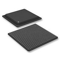
XC6SLX100-2FGG484C Xilinx Inc, XC6SLX100-2FGG484C Datasheet - Page 47

XC6SLX100-2FGG484C
Manufacturer Part Number
XC6SLX100-2FGG484C
Description
FPGA Spartan®-6 Family 101261 Cells 45nm (CMOS) Technology 1.2V 484-Pin FBGA
Manufacturer
Xilinx Inc
Series
Spartan® 6 LXr
Specifications of XC6SLX100-2FGG484C
Package
484FBGA
Family Name
Spartan®-6
Device Logic Cells
101261
Device Logic Units
63288
Number Of Registers
126576
Typical Operating Supply Voltage
1.2 V
Maximum Number Of User I/os
326
Ram Bits
4939776
Number Of Logic Elements/cells
101261
Number Of Labs/clbs
7911
Total Ram Bits
4939776
Number Of I /o
326
Voltage - Supply
1.14 V ~ 1.26 V
Mounting Type
Surface Mount
Operating Temperature
0°C ~ 85°C
Package / Case
484-BBGA
No. Of Logic Blocks
15822
No. Of Macrocells
101261
Family Type
Spartan-6
No. Of Speed Grades
2
No. Of I/o's
326
Clock Management
DCM, PLL
Rohs Compliant
Yes
Lead Free Status / RoHS Status
Lead free / RoHS Compliant
Number Of Gates
-
Lead Free Status / RoHS Status
Lead free / RoHS Compliant
Available stocks
Company
Part Number
Manufacturer
Quantity
Price
Company:
Part Number:
XC6SLX100-2FGG484C
Manufacturer:
ST
Quantity:
4 450
Company:
Part Number:
XC6SLX100-2FGG484C
Manufacturer:
Xilinx Inc
Quantity:
10 000
Table 46: Configuration Switching Characteristics
DS162 (v2.0) March 31, 2011
Preliminary Product Specification
Notes:
1.
2.
3.
4.
T
SPI Master Flash Mode Programming Switching
T
T
T
T
CCLK Output (Master Modes)
T
T
F
F
CCLK Input (Slave Modes)
T
T
USERCCLK Input
T
T
F
BPIDCC
SPIDCC
SPIICCK
SPICCM
SPICCFC
MCCKL
MCCKH
MCCK
MCCKTOL
SCCKL
SCCKH
USERCCLKL
USERCCLKH
USERCCLK
Maximum frequency and setup/hold timing parameters are for 3.3V and 2.5V configuration voltages.
To support longer delays in configuration, use the design solutions described in the Spartan-6 FPGA Configuration User Guide.
BPI mode is not supported in:
•
•
•
Only during configuration, the last edge is determined by a weak pull-up/pull-down resistor in the I/O.
Symbol
/T
/T
LX4, LX25, or LX25T devices
LX9 devices in the TQG144 package
LX9 or LX16 devices in the CPG196 package.
BPICCD
SPIDCCD
Setup/Hold on D[15:0] data input pins
DIN, MISO0, MISO1, MISO2, MISO3, Setup/Hold
before/after the rising CCLK edge
Master SPI CCLK (output) delay
MOSI clock to out
CSO_B clock to out
Master CCLK clock duty cycle Low
Master CCLK clock duty cycle High
Maximum frequency, serial mode (Master Serial/SPI)
All devices
Maximum frequency, parallel mode (Master
SelectMAP/BPI)
XC6SLX4, XC6SLX9, XC6SLX16, XC6SLX25,
XC6SLX25T, XC6SLX45, XC6SLX45T, XC6SLX75, and
XC6SLX75T
Maximum frequency, parallel mode (Master
SelectMAP/BPI)
XC6SLX100 and XC6SLX100T in x8 mode,
XC6SLX150, and XC6SLX150T
Maximum frequency, parallel mode (Master
SelectMAP/BPI)
XC6SLX100 and XC6SLX100T in x16 mode
Frequency Tolerance, master mode
Slave CCLK clock minimum Low time
Slave CCLK clock minimum High time
USERCCLK clock minimum Low time
USERCCLK clock minimum High time
Maximum USERCCLK frequency
Description
(1)
www.xilinx.com
Spartan-6 FPGA Data Sheet: DC and Switching Characteristics
(Cont’d)
5.0/1.0
5.0/1.0
0.4/7.0
±50
13
16
40
40
40
35
12
12
40
-3
5
5
5.0/1.0
5.0/1.0
0.4/7.0
Speed Grade
-3N
±50
13
16
40
40
40
35
12
12
40
5
5
40/60
40/60
5.0/1.0
5.0/1.0
0.4/7.0
±50
13
16
40
40
40
35
12
12
40
-2
5
5
0.4/10.0 µs, Min/Max
6.0/2.0
7.0/1.0
±50
-1L
19
26
30
25
20
20
16
16
30
8
8
%, Min/Max
%, Min/Max
MHz, Max
MHz, Max
MHz, Max
MHz, Max
MHz, Max
ns, Max
ns, Max
ns, Min
ns, Min
ns, Min
ns, Min
ns, Min
ns, Min
Units
%
47


